ZHCSGP5C August 2017 – February 2022 TIC12400-Q1
PRODUCTION DATA
- 1 特性
- 2 应用
- 3 说明
- 4 Revision History
- 5 Pin Configuration and Functions
- 6 Specifications
- 7 Parameter Measurement Information
-
8 Detailed Description
- 8.1 Overview
- 8.2 Functional Block Diagram
- 8.3
Feature Description
- 8.3.1 VS Pin
- 8.3.2 VDD Pin
- 8.3.3 Device Initialization
- 8.3.4 Device Trigger
- 8.3.5 Device Reset
- 8.3.6 VS Under-Voltage (UV) Condition
- 8.3.7 VS Over-Voltage (OV) Condition
- 8.3.8 Switch Inputs Settings
- 8.3.9 Interrupt Generation and INT Assertion
- 8.3.10 Temperature Monitor
- 8.3.11 Parity Check and Parity Generation
- 8.3.12 Cyclic Redundancy Check (CRC)
- 8.4 Device Functional Modes
- 8.5 Programming
- 8.6 Register Maps
- 8.7 Programming Guidelines
- 9 Application Information Disclaimer
- 10Power Supply Recommendations
- 11Layout
- 12Device and Documentation Support
- 13Mechanical, Packaging, and Orderable Information
8.4.2.1 Standard Polling
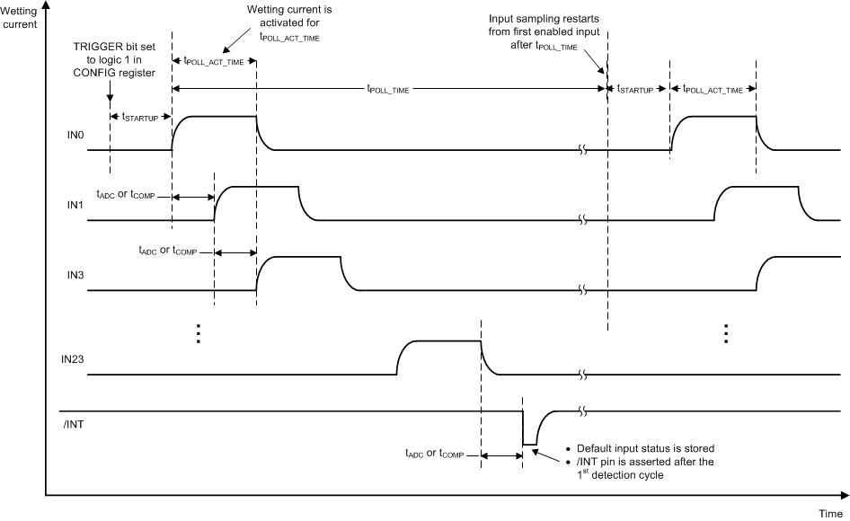
In standard polling mode, wetting current is applied to each input for a pre-programmed polling active time between 64 μs and 2048 μs, set by the POLL_ACT_TIME bits in the CONFIG register. At the end of the wetting current application, the input voltage is sampled by the comparator (if input is configured as comparator input mode) or the ADC (if input is configured as ADC input mode). Each input is cycled through in sequential order from IN0 to IN23. Sampling is repeated at a frequency from 2 ms to 4096 ms, set by the POLL_TIME bits in the CONFIG register. Wetting currents are applied to closed switches only during the polling active time; hence, the overall system current consumption can be greatly reduced.
Similar to continuous mode, after the first polling cycle, the switch status of each input (below or above detection threshold) is stored in registers (IN_STAT_COMP for comparator inputs and IN_STAT_ADC0 to IN_STAT_ADC1 for ADC inputs) to be used as the default state for subsequent polling cycles. The digital values (if the input is configured as ADC input mode) are stored in the registers ANA_STAT0 to ANA_STAT11. The INT pin is asserted low to notify the microcontroller that the default switch status is ready to be read. The SSC bit in INT_STAT register and the SPI status flag SSC are also asserted to logic 1. The INT_STAT register is cleared and INT pin de-asserted if a SPI READ command is issued to the register. Note the interrupt is always generated after the 1st polling cycle (after the TRIGGER bit in register CONFIG is set to logic 1). In subsequent polling cycles the interrupt is generated only if switch status change is detected.
An example of the timing diagram of the polling mode operation is shown in Figure 8-12.
 Figure 8-12 An Example of the Polling Sequence in Standard Polling Mode
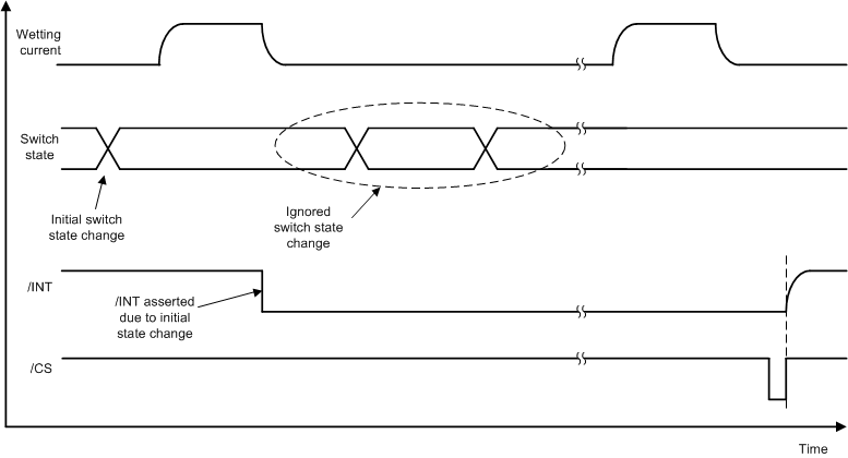
If the switch position changes between two active polling times, no interrupt will be generated and the status registers (IN_STAT_COMP for comparator inputs and IN_STAT_ADC0 to IN_STAT_ADC1 for ADC inputs) will not reflect such a change. An example is shown in Figure 8-13.
 Figure 8-13 Example for Ignored Switch Position Change Between 2 Wetting Current Cycles