ZHCSGP5C August 2017 – February 2022 TIC12400-Q1
PRODUCTION DATA
- 1 特性
- 2 应用
- 3 说明
- 4 Revision History
- 5 Pin Configuration and Functions
- 6 Specifications
- 7 Parameter Measurement Information
-
8 Detailed Description
- 8.1 Overview
- 8.2 Functional Block Diagram
- 8.3
Feature Description
- 8.3.1 VS Pin
- 8.3.2 VDD Pin
- 8.3.3 Device Initialization
- 8.3.4 Device Trigger
- 8.3.5 Device Reset
- 8.3.6 VS Under-Voltage (UV) Condition
- 8.3.7 VS Over-Voltage (OV) Condition
- 8.3.8 Switch Inputs Settings
- 8.3.9 Interrupt Generation and INT Assertion
- 8.3.10 Temperature Monitor
- 8.3.11 Parity Check and Parity Generation
- 8.3.12 Cyclic Redundancy Check (CRC)
- 8.4 Device Functional Modes
- 8.5 Programming
- 8.6 Register Maps
- 8.7 Programming Guidelines
- 9 Application Information Disclaimer
- 10Power Supply Recommendations
- 11Layout
- 12Device and Documentation Support
- 13Mechanical, Packaging, and Orderable Information
8.3.8.4 Thresholds Adjustment
When an input is configured as comparator input mode, the threshold level for interrupt generation can be programmed by setting the THRES_COMP register. The threshold level settings can be set for each individual input groups and each group consists of 4 inputs. Four threshold levels are available: 2 V, 2.7 V, 3 V, and 4 V.
When an input is configured as ADC input mode the threshold level for interrupt generation can be configured from 0 to 1023 different levels by setting the THRES_CFG1 to THRES_CFG2 registers. One threshold level can be programmed individually for each of the inputs from IN0 to IN11. Additionally, one common threshold, shared between inputs IN0 to IN11, can be programmed by configuring the THRES_COM bits in register MATRIX. The common threshold acts independently from the threshold THRES0 to THRES7. Inputs IN12 to IN17 use 2 preset threshold levels (THRES2A and THRES2B). Inputs 18 to 22 use 3 preset threshold levels (THRES3A, THRES3B, and THRES3C). Input 23 uses 5 preset threshold levels (THRES3A, THRES3B, THRES3C, THRES8, and THRES9).
When multiple threshold settings are used for ADC inputs, the thresholds levels need to be configured properly. Use the rules below (see Table 8-2) when setting up the threshold levels:
| INPUT | PROPER THRESHOLD CONFIGURATION |
|---|---|
| IN12 to IN17 | THRES2B ≥ THRES2A |
| IN18 to IN22 | THRES3C ≥ THRES3B ≥ THRES3A |
| IN23 | THRES9 ≥ THRES8 ≥ THRES3C ≥ THRES3B ≥ THRES3A |
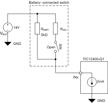
Remember to use caution when setting up the threshold for switches that are connected externally to the battery as there is a finite voltage drop (as high as VCSI_DROP_OPEN for 10 mA and 15 mA settings) across the current sinks. Therefore, even for an open switch, the voltage on the INx pin can be as high as VCSI_DROP_OPEN and the detection threshold shall be configured above it. It shall also be noted that a lower wetting current sink setting may not be strong enough to pull the INx pin close to ground in the presence of a leaky open external switch, as illustrated in the diagram below (see Figure 8-3). In this example, the external switch, although in the open state, has large leakage current and can be modelled as an equivalent resistor (RDIRT) of 5 kΩ. The 2 mA current sink is only able to pull the INx pin voltage down to 4 V, even if the switch is in the open state.
 Figure 8-3 Example Showing the Calculation of the INx Pin Voltage for A Leaky Battery-Connected Switch
It is possible to configure an input to ADC input mode, instead of comparator input mode, to monitor single-threshold digital switches. The following programming procedure is recommended under such configuration:
| INPUT | RECOMMENDED THRESHOLD CONFIGURATION |
|---|---|
| IN0 to IN11 | Configure the desired threshold to one of the settings from THRES0 to THRES7 and map it accordingly |
| IN12 to IN17 |
|
| IN18 to IN22 |
|
| IN23 |
|