ZHCSLJ5D February 2022 – March 2023 TIOL112 , TIOL1123 , TIOL1125
PRODUCTION DATA
- 1 特性
- 2 应用
- 3 说明
- 4 Revision History
- 5 Pin Configuration and Functions
- 6 Specifications
- 7 Parameter Measurement Information
-
8 Detailed Description
- 8.1 Overview
- 8.2 Functional Block Diagrams
- 8.3
Feature Description
- 8.3.1 Wake-Up Detection
- 8.3.2 Current Limit Configuration
- 8.3.3 Current Fault Detection, Indication and Auto Recovery
- 8.3.4 Thermal Warning, Thermal Shutdown
- 8.3.5 Fault Reporting (NFAULT)
- 8.3.6 Transceiver Function Tables
- 8.3.7 The Integrated Voltage Regulator (LDO)
- 8.3.8 Reverse Polarity Protection
- 8.3.9 Integrated Surge Protection and Transient Waveform Tolerance
- 8.3.10 Power Up Sequence (TIOL112)
- 8.3.11 Undervoltage Lock-Out (UVLO)
- 8.4 Device Functional Modes
- 9 Application and Implementation
- 10Device and Documentation Support
- 11Mechanical, Packaging, and Orderable Information
封装选项
机械数据 (封装 | 引脚)
- YAH|12
- DRC|10
散热焊盘机械数据 (封装 | 引脚)
- DRC|10
订购信息
8.3.9 Integrated Surge Protection and Transient Waveform Tolerance
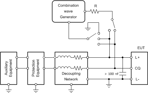
The L+ and CQ pins of the device are capable of withstanding up to 1.2 kV of 1.2/50 – 8/20 μs IEC 61000-4-5 surge with a source impedance of 500 Ω. The surge testing should be performed with a minimum 100 nF supply decoupling capacitor between L+ and L-, and 1 µF between VCC_IN/OUT and L-.
External TVS diodes may be required for higher transient protection levels. The system designer should make sure the maximum clamping voltage of the external diodes is < 65 V at the desired current level. The device is capable of withstanding up to ±70-V transient pulses < 100 µs.

1.2/50 – 8/20 µs CWG
R = 500 Ω
Figure 8-6 Surge Test Setup