ZHCSMU4B february 2022 – june 2023 TIOS102 , TIOS1023 , TIOS1025
PRODUCTION DATA
- 1
- 1 特性
- 2 应用
- 3 说明
- 4 Revision History
- 5 Pin Configuration and Functions
- 6 Specifications
- 7 Parameter Measurement Information
-
8 Detailed Description
- 8.1 Overview
- 8.2 Functional Block Diagrams
- 8.3
Feature Description
- 8.3.1 Current Limit Configuration
- 8.3.2 Current Fault Detection, Indication and Auto Recovery
- 8.3.3 Thermal Warning, Thermal Shutdown
- 8.3.4 Fault Reporting (NFAULT)
- 8.3.5 Device Function Tables
- 8.3.6 The Integrated Voltage Regulator (LDO)
- 8.3.7 Reverse Polarity Protection
- 8.3.8 Integrated Surge Protection and Transient Waveform Tolerance
- 8.3.9 Power Up Sequence
- 8.3.10 Undervoltage Lock-Out (UVLO)
- 8.4 Device Functional Modes
- 9 Application Information Disclaimer
- 10Power Supply Recommendations
- 11Layout
- 12Device and Documentation Support
- 13Mechanical, Packaging, and Orderable Information
封装选项
机械数据 (封装 | 引脚)
- YAH|12
- DRC|10
散热焊盘机械数据 (封装 | 引脚)
- DRC|10
订购信息
7 Parameter Measurement Information
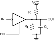
 Figure 7-1 Test
Circuit for Driver Switching
 Figure 7-2 Waveforms
for Driver Output Switching Measurements
 Figure 7-3 Waveforms
for Driver Enable or Disable Time Measurements