ZHCSA03C july 2012 – november 2020 TL1431-SP
PRODUCTION DATA
- 1
- 1 特性
- 2 应用
- 3 说明
- 4 Revision History
- 5 Pin Configuration and Functions
- 6 Specifications
- 7 Parameter Measurement Information
- 8 Detailed Description
- 9 Application and Implementation
- 10Power Supply Recommendations
- 11Layout
- 12Device and Documentation Support
- 13Mechanical, Packaging, and Orderable Information
6.6 Typical Characteristics
Data at high and low temperatures are applicable only within the recommended operating free-air temperature ranges of the various devices.
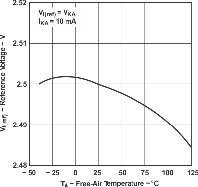 Figure 6-1 Reference
Voltage vs Free-Air Temperature
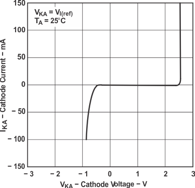 Figure 6-3 Cathode Current
vs Cathode Voltage
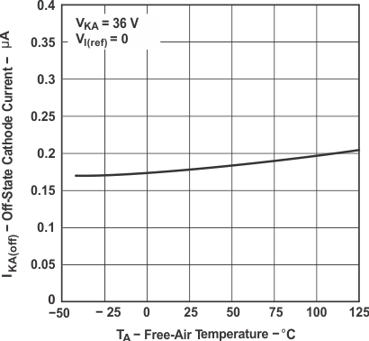 Figure 6-5 Off-State
Cathode Current vs Free-Air Temperature
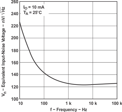 Figure 6-7 Equivalent
Input-Noise Voltage vs Frequency
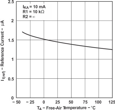 Figure 6-2 Reference
Current vs Free-Air Temperature
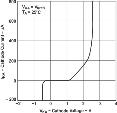 Figure 6-4 Cathode Current
vs Cathode Voltage
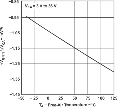 Figure 6-6 Ratio of Delta
Reference Voltage to Delta Cathode Voltage vs Free-Air Temperature
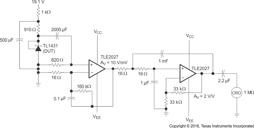
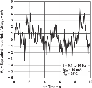 Figure 6-8 Equivalent
Input-Noise Voltage Over a 10-s Period
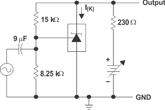
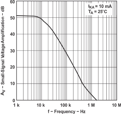 Figure 6-10 Small-Signal
Voltage Amplification vs Frequency
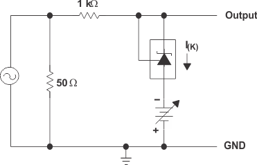
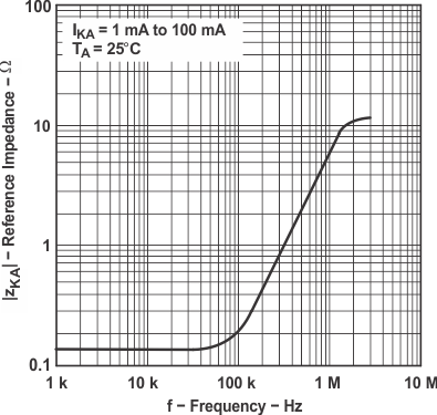 Figure 6-12 Reference
Impedance vs Frequency
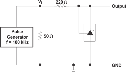
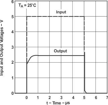 Figure 6-14 Pulse
Response
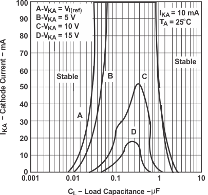
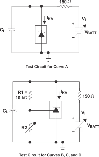
A. The areas under the curves represent
conditions that may cause the device to oscillate. For curves B, C; and D, R2; and V+
are adjusted to establish the initial VKA and IKA conditions, with
CL = 0. VBATT and CL then are adjusted to determine
the ranges of stability.
Figure 6-16 Stability
Boundary Conditions