ZHCSKJ6 December 2019 TL16C750E
PRODUCTION DATA.
- 1 特性
- 2 应用
- 3 说明
- 4 修订历史记录
- 5 说明 (续)
- 6 Pin Configuration and Functions
- 7 Specifications
- 8 Parameter Measurement Information
-
9 Detailed Description
- 9.1 Overview
- 9.2 Functional Block Diagrams
- 9.3
Feature Description
- 9.3.1 UART Modes
- 9.3.2 Trigger Levels
- 9.3.3 Hardware Flow Control
- 9.3.4 Auto-RTS
- 9.3.5 Auto-CTS
- 9.3.6 Software Flow Control
- 9.3.7 Software Flow Control Example
- 9.3.8 Reset
- 9.3.9 Interrupts
- 9.3.10 Interrupt Mode Operation
- 9.3.11 Polled Mode Operation
- 9.3.12 Break and Timeout Conditions
- 9.3.13 Programmable Baud Rate Generator with Fractional Divisor
- 9.3.14 Fractional Divisor
- 9.4 Device Functional Modes
- 9.5
Register Maps
- 9.5.1 Registers Operations
- 9.5.2 Receiver Holding Register (RHR)
- 9.5.3 Transmit Holding Register (THR)
- 9.5.4 FIFO Control Register (FCR)
- 9.5.5 Line Control Register (LCR)
- 9.5.6 Line Status Register (LSR)
- 9.5.7 Modem Control Register (MCR)
- 9.5.8 Modem Status Register (MSR)
- 9.5.9 Interrupt Enable Register (IER)
- 9.5.10 Interrupt Identification Register (IIR)
- 9.5.11 Enhanced Feature Register (EFR)
- 9.5.12 Divisor Latches (DLL, DLH, DLF)
- 9.5.13 Transmission Control Register (TCR)
- 9.5.14 Trigger Level Register (TLR)
- 9.5.15 FIFO Ready Register
- 9.5.16 Alternate Function Register (AFR)
- 9.5.17 RS-485 Mode
- 9.5.18 IrDA Overview
- 9.5.19 IrDA Encoder Function
- 10Application and Implementation
- 11Power Supply Recommendations
- 12Layout
- 13器件和文档支持
- 14机械、封装和可订购信息
9.5.19 IrDA Encoder Function
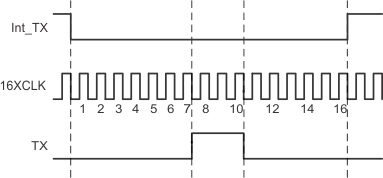
Serial data from a UART is encoded to transmit data to the optoelectronics. While the serial data input to this block (Int_TX) is high, the output (TX) is always low, and the counter used to form a pulse on TX is continuously cleared. After Int_TX resets to 0, TX rises on the falling edge of the 7th 16XCLK. On the falling edge of the 10th 16XCLK pulse, TX falls, creating a 3-clock-wide pulse. While Int_TX stays low, a pulse is transmitted during the seventh to tenth clocks of each 16-clock bit cycle.
 Figure 35. IrDA-SIR Encoding Scheme – Detailed Timing Diagram
  Figure 36. Encoding Scheme – Macro View
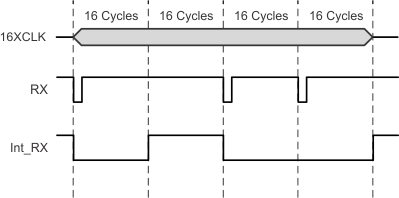
 After reset, Int_RX is high and the 4-bit counter is cleared. When a falling edge is detected on RX, Int_RX falls on the next rising edge of 16XCLK with sufficient setup time. Int_RX stays low for 16 cycles (16XCLK) and then returns to high as required by the IrDA specification. As long as no pulses (falling edges) are detected on RX, Int_RX remains high.
 Figure 37. IrDA-SIR Decoding Scheme – Detailed Timing Diagram
  Figure 38. IrDA-SIR Decoding Scheme – Macro View
 It is possible for jitter or slight frequency differences to cause the next falling edge on RX to be missed for one 16XCLK cycle. In that case, a 1-clock-wide pulse appears on Int_RX between consecutive 0s. It is important for the UART to strobe Int_RX in the middle of the bit time to avoid latching this 1-clock-wide pulse. The TL16C750E UART already strobes incoming serial data at the proper time. Otherwise, note that data is required to be framed by a leading 0 and a trailing 1. The falling edge of that first 0 on Int_RX synchronizes the read strobe. The strobe occurs on the 8th 16XCLK pulse after the Int_RX falling edge and once every 16 cycles thereafter until the stop bit occurs.
 Figure 39. Timing Causing 1-Clock-Wide Pulse Between Consecutive Ones
  Figure 40. Recommended Strobing for Decoded Data
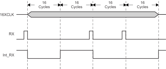
 The TL16C750E device can decode positive pulses on RX. The timing is different, but the variation is invisible to the UART. The decoder, which works from the falling edge, now recognizes a 0 on the trailing edge of the pulse rather than on the leading edge. As long as the pulse duration is fairly constant, as defined by the specification, the trailing edges should also be 16 clock cycles apart and data can readily be decoded. The 0 appears on Int_RX after the pulse rather than at the start of it.
 Figure 41. Positive RX Pulse Decode – Detailed View
  Figure 42. Positive RX Pulse Decode – Macro View