ZHCSX73C August 2006 – October 2024
PRODUCTION DATA
- 1
- 1 特性
- 2 应用
- 3 说明
- 4 Pin Configuration and Functions
-
5 Specifications
- 5.1 Absolute Maximum Ratings
- 5.2 ESD Ratings
- 5.3 Recommended Operating Conditions
- 5.4 Thermal Information
- 5.5 Reference Section Electrical Characteristics
- 5.6 Oscillator Section Electrical Characteristics
- 5.7 Error-Amplifier Section Electrical Characteristics
- 5.8 Current-Sense Section Electrical Characteristics
- 5.9 Output Section Electrical Characteristics
- 5.10 Undervoltage-Lockout Section Electrical Characteristics
- 5.11 Pulse-Width Modulator Section Electrical Characteristics
- 5.12 Supply Voltage Electrical Characteristics
- 5.13 Typical Characteristics
- 6 Detailed Description
- 7 Application and Implementation
- 8 Device and Documentation Support
- 9 Revision History
- 10Mechanical, Packaging, and Orderable Information
封装选项
机械数据 (封装 | 引脚)
散热焊盘机械数据 (封装 | 引脚)
订购信息
7.2 Shutdown Technique
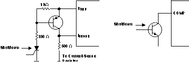
The PWM controller (see Figure 7-4) can be shut down by two methods: either raise the voltage at ISENSE above 1 V or pull the COMP terminal below a voltage two diode drops above ground. Either method causes the output of the PWM comparator to be high (refer to block diagram). The PWM latch is reset dominant so that the output remains low until the next clock cycle after the shutdown condition at the COMP or ISENSE terminal is removed. In one example, an externally latched shutdown can be accomplished by adding an SCR that resets by cycling VCC below the lower UVLO threshold. At this point, the reference turns off, allowing the SCR to reset.
 Figure 7-4 Shutdown Techniques
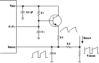
A fraction of the oscillator ramp can be summed resistively with the current-sense signal to provide slope compensation for converters requiring duty cycles over 50% (see Figure 7-5). Note that capacitor C forms a filter with R2 to suppress the leading-edge switch spikes.
 Figure 7-5 Slope Compensation