SLVS052I April 1988 – September 2016 TL594
PRODUCTION DATA.
- 1 Features
- 2 Applications
- 3 Description
- 4 Revision History
- 5 Pin Configuration and Functions
- 6 Specifications
- 7 Parameter Measurement Information
- 8 Detailed Description
-
9 Application and Implementation
- 9.1 Application Information
- 9.2 Typical Application
- 10Power Supply Recommendations
- 11Layout
- 12Device and Documentation Support
- 13Mechanical, Packaging, and Orderable Information
封装选项
请参考 PDF 数据表获取器件具体的封装图。
机械数据 (封装 | 引脚)
- PW|16
- NS|16
- N|16
- D|16
散热焊盘机械数据 (封装 | 引脚)
订购信息
1 Features
- Complete PWM Power-Control Circuitry
- Uncommitted Outputs for 200-mA Sink or Source Current
- Output Control Selects Single-Ended or Push-Pull Operation
- Internal Circuitry Prohibits Double Pulse at Either Output
- Variable Dead Time Provides Control Over Total Range
- Internal Regulator Provides a Stable 5-V Reference Supply Trimmed to 1%
- Circuit Architecture Allows Easy Synchronization
- Undervoltage Lockout (UVLO) for Low-VCC Conditions
2 Applications
- White Goods
- Power Supplies: AC/DC, Isolated,
With PFC, > 90 W - Server PSUs
- Solar Micro-Inverters
- Power Supplies: AC/DC, Isolated,
No PFC, < 90 W - Power: Telecom/Server AC/DC Supplies
- Solar Power Inverters
3 Description
The TL594 device incorporates all the functions required in the construction of a pulse-width-modulation (PWM) control circuit on a single chip. Designed primarily for power-supply control, this device offers the systems engineer the flexibility to tailor the power-supply control circuitry to a specific application.
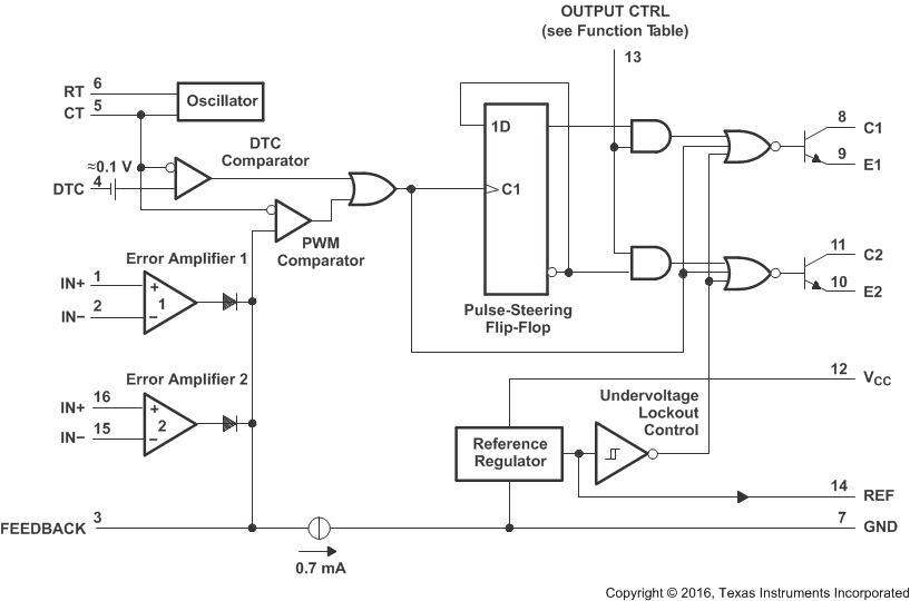
The TL594 device contains two error amplifiers, an on-chip adjustable oscillator, a dead-time control (DTC) comparator, a pulse-steering control flip-flop, a 5-V regulator with a precision of 1%, an undervoltage lockout control circuit, and output control circuitry.
The uncommitted output transistors provide either common-emitter or emitter-follower output capability. Each device provides for push-pull or single-ended output operation, with selection by means of the output-control function. The architecture of these devices prohibits the possibility of either output being pulsed twice during push-pull operation. The undervoltage lockout control circuit locks the outputs off until the internal circuitry is operational.
Device Information
| PART NUMBER | PACKAGE | BODY SIZE (NOM) |
|---|---|---|
| TL594D | SOIC (16) | 9.90 mm × 3.91 mm |
| TL594N | PDIP (16) | 19.30 mm × 6.35 mm |
| TL594NS | SO (16) | 10.30 mm × 5.30 mm |
| TL594PW | TSSOP (16) | 5.00 mm × 4.40 mm |
