SLVS052I April 1988 – September 2016 TL594
PRODUCTION DATA.
- 1 Features
- 2 Applications
- 3 Description
- 4 Revision History
- 5 Pin Configuration and Functions
- 6 Specifications
- 7 Parameter Measurement Information
- 8 Detailed Description
-
9 Application and Implementation
- 9.1 Application Information
- 9.2 Typical Application
- 10Power Supply Recommendations
- 11Layout
- 12Device and Documentation Support
- 13Mechanical, Packaging, and Orderable Information
封装选项
请参考 PDF 数据表获取器件具体的封装图。
机械数据 (封装 | 引脚)
- PW|16
- NS|16
- N|16
- D|16
散热焊盘机械数据 (封装 | 引脚)
订购信息
9 Application and Implementation
NOTE
Information in the following applications sections is not part of the TI component specification, and TI does not warrant its accuracy or completeness. TI’s customers are responsible for determining suitability of components for their purposes. Customers should validate and test their design implementation to confirm system functionality.
9.1 Application Information
The TL594 device contains an adjustable oscillator, a dead-time control comparator, a pulse-steering flip flop, two error amplifiers, and a 5-V regulator. The TL594 device can be used for a wide variety of switching converter applications over a frequency range of 1 Hz to 300 kHz, where the oscillation frequency is set by the RT and CT values. For additional information regarding designing switching voltage regulators with the TL594, see Designing Switching Voltage Regulators With the TL494.
9.2 Typical Application
This design example uses the TL594 to create a 5-V, 10-A power supply. This application is from Designing Switching Voltage Regulators With the TL494.
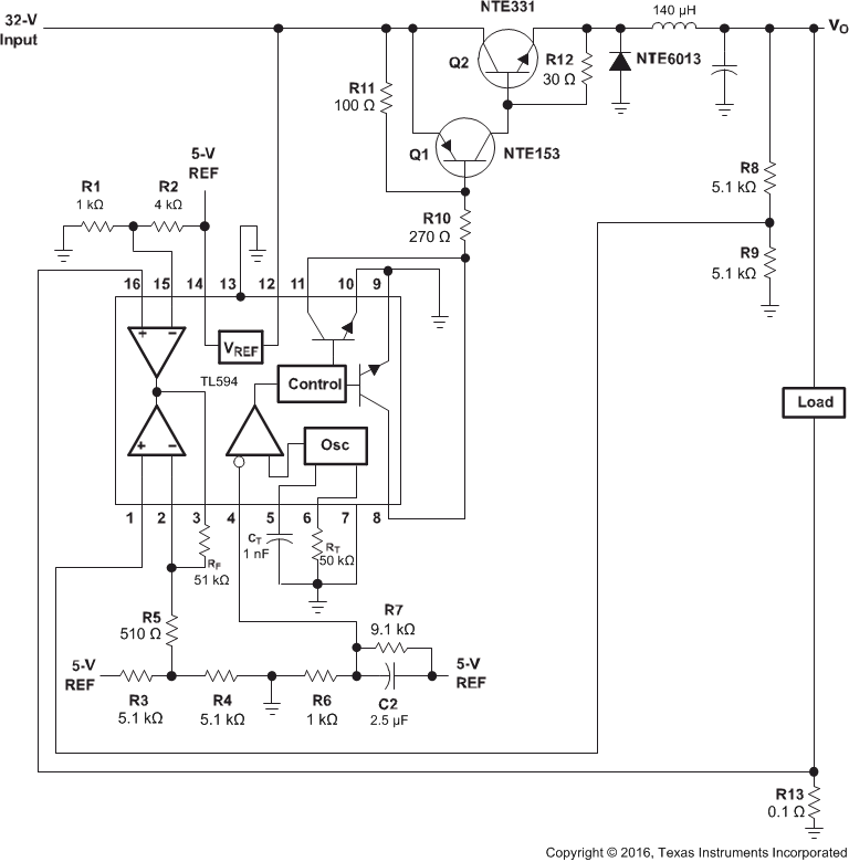 Figure 7. 32-V to 5-V, 10-A Power Supply Application
9.2.1 Design Requirements
- VI = 32 V
- VO = 5 V
- IO = 10 A
- fOSC = 20-kHz switching frequency
- VR = 20-mV peak-to-peak (VRIPPLE)
- ΔIL = 1.5-A inductor current change
9.2.2 Detailed Design Procedure
9.2.2.1 Input Power Source
The 32-V dc power source for this supply uses a 120-V input, 24-V output transformer rated at 75 VA. The 24-V secondary winding feeds a full-wave bridge rectifier, followed by a current-limiting resistor (0.3 Ω) and two filter capacitors (see Figure 8).
 Figure 8. Input Power Source
The output voltage and current are determined by Equation 6 and Equation 7.


The 3-A, 50-V full-wave bridge rectifier meets these calculated conditions. Figure 7 shows the switching and control sections.
9.2.2.2 Control Circuits
9.2.2.2.1 Oscillator
Connecting an external capacitor and resistor to pins 5 and 6 controls the TL594 oscillator frequency. The oscillator is set to operate at 20 kHz, using the component values calculated by Equation 8 and Equation 9.

Choose CT = 0.001 µF and calculate RT with Equation 9.

9.2.2.2.2 Error Amplifier
The error amplifier compares a sample of the 5-V output to the reference and adjusts the PWM to maintain a constant output current (see Figure 9).
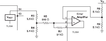 Figure 9. Error-Amplifier Section
The TL594 internal 5-V reference is divided to 2.5 V by R3 and R4. The output-voltage error signal also is divided to 2.5 V by R8 and R9. If the output must be regulated to exactly 5 V, a 10-kΩ potentiometer can be used in place of R8 to provide an adjustment.
To increase the stability of the error-amplifier circuit, the output of the error amplifier is fed back to the inverting input through RT, reducing the gain to 101.
9.2.2.2.3 Current-Limiting Amplifier
The power supply was designed for a 10-A load current and an IL swing of 1.5 A; therefore, the short-circuit current is calculated as Equation 10.

Figure 10 shows the current-limiting circuit.
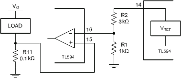 Figure 10. Current-Limiting Circuit
Resistors R1 and R2 set the reference of about 1 V on the inverting input of the current-limiting amplifier. Resistor R13, in series with the load, applies 1 V to the noninverting terminal of the current-limiting amplifier when the load current reaches 10 A. The output-pulse width is reduced accordingly. The value of R13 is calculated as Equation 11.

9.2.2.2.4 Soft Start
To reduce stress on the switching transistors at start-up, the start-up surge that occurs as the output filter capacitor charges must be reduced. The availability of the dead-time control makes implementation of a soft-start circuit relatively simple (see Figure 11).
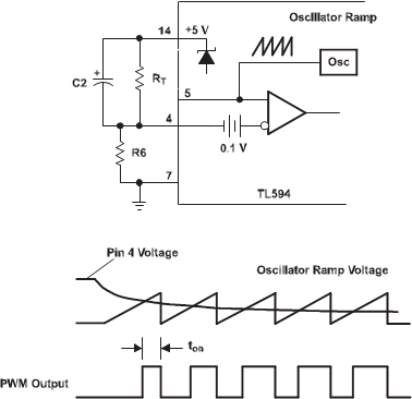 Figure 11. Soft-Start Circuit
The soft-start circuit allows the pulse width at the output to increase slowly (see Figure 11) by applying a negative slope waveform to the dead-time control input (pin 4).
Initially, capacitor C2 forces the dead-time control input to follow the 5-V regulator, which disables the outputs (100% dead time). As the capacitor charges through R6, the output pulse width slowly increases until the control loop takes command. With a resistor ratio of 1:10 for R6 and R7, the voltage at pin 4 after start-up is 0.1 × 5 V, or 0.5 V.
The soft-start time generally is in the range of 25 to 100 clock cycles. If 50 clock cycles at a 20-kHz switching rate is selected, the soft-start time is calculated as Equation 12.

The value of the capacitor then is determined with Equation 13.

This helps eliminate any false signals that might be created by the control circuit as power is applied.
9.2.2.2.5 Setting the Dead Time
The primary function of the dead-time control is to control the minimum off time of the output of the TL594 device. The dead-time control input provides control from 5% to 100% dead time. The TL594 device can be tailored to the specific power transistor switches that are used, to ensure that the output transistors never experience a common on-time. Figure 12 shows the bias circuit for the basic function.
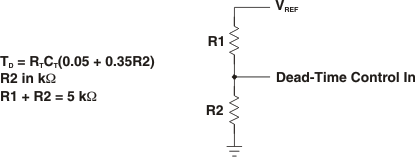 Figure 12. Setting Dead Time
9.2.2.3 Inductor Calculations
Figure 13 shows the switching circuit used.
 Figure 13. Switching Circuit
The size of the inductor (L) required is:
| d | = | duty cycle = VO/VI = 5 V/32 V = 0.156 |
| f | = | 20 kHz (design objective) |
| ton | = | time on (S1 closed) = (1/f) × d = 7.8 µs |
| toff | = | time off (S1 open) = (1/f) – ton = 42.2 µs |
| L | ≉ | (VI – VO ) × ton/ΔIL |
| ≉ | [(32 V – 5 V) × 7.8 µs]/1.5 A | |
| ≉ | 140.4 µH |
9.2.2.4 Output Capacitance Calculations
Once the filter inductor has been calculated, the value of the output filter capacitor is calculated to meet the output ripple requirements. An electrolytic capacitor can be modeled as a series connection of an inductance, a resistance, and a capacitance. To provide good filtering, the ripple frequency must be far below the frequencies at which the series inductance becomes important. So, the two components of interest are the capacitance and the effective series resistance (ESR). The maximum ESR is calculated with Equation 14 according to the relation between the specified peak-to-peak ripple voltage and the peak-to-peak ripple current.

The minimum capacitance of C3 necessary to maintain the VO ripple voltage at less than the 100-mV design objective is calculated according to Equation 15.

A 220-mF, 60-V capacitor is selected because it has a maximum ESR of 0.074 Ω and a maximum ripple current of 2.8 A.
9.2.2.5 Transistor Power-Switch Calculations
The transistor power switch was constructed with an NTE153 pnp drive transistor and an NTE331 npn output transistor. These two power devices were connected in a pnp hybrid Darlington circuit configuration (see Figure 14).
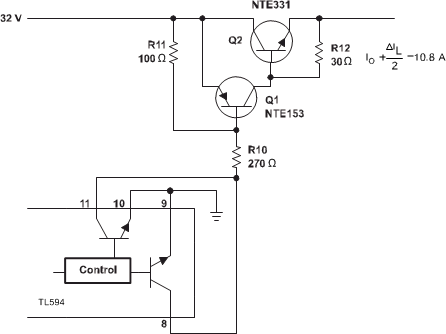 Figure 14. Power-Switch Section
The hybrid Darlington circuit must be saturated at a maximum output current of IO + ΔIL/2 or 10.8 A. The Darlington hFE at 10.8 A must be high enough not to exceed the 250-mA maximum output collector current of the TL594. Based on published NTE153 and NTE331 specifications, the required power-switch minimum drive was calculated by Equation 16 through Equation 18 to be 144 mA.


The value of R10 was calculated by Equation 19.

Based on these calculations, the nearest standard resistor value of 220 Ω was selected for R10. Resistors R11 and R12 permit the discharge of carriers in switching transistors when they are turned off.
The power supply described demonstrates the flexibility of the TL594 PWM control circuit. This power-supply design demonstrates many of the power-supply control methods provided by the TL594, as well as the versatility of the control circuit.
9.2.3 Application Curve
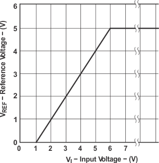 Figure 15. Reference Voltage vs Input Voltage