ZHCSUM8I September   2008  – May 2024 TL720M05-Q1

PRODMIX  

  1.   1
  2. 特性
  3. 应用
  4. 说明
  5. Pin Configuration and Functions
  6. Specifications
    1. 5.1 Absolute Maximum Ratings
    2. 5.2 ESD Ratings
    3. 5.3 Recommended Operating Conditions
    4. 5.4 Thermal Information
    5. 5.5 Electrical Characteristics
    6. 5.6 Typical Characteristics
  7. Parameter Measurement Information
  8. Detailed Description
    1. 7.1 Overview
    2. 7.2 Functional Block Diagrams
    3. 7.3 Feature Description
      1. 7.3.1 Undervoltage Lockout
      2. 7.3.2 Thermal Shutdown
      3. 7.3.3 Current Limit
    4. 7.4 Device Functional Modes
      1. 7.4.1 Normal Operation
      2. 7.4.2 Dropout Operation
      3. 7.4.3 Disabled
  9. Application and Implementation
    1. 8.1 Application Information
      1. 8.1.1 Input and Output Capacitor Selection
        1. 8.1.1.1 Legacy Chip Capacitor Selection
        2. 8.1.1.2 New Chip Output Capacitor
        3. 8.1.1.3 New Chip Input Capacitor
      2. 8.1.2 Dropout Voltage
      3. 8.1.3 Reverse Current
      4. 8.1.4 Power Dissipation (PD)
        1. 8.1.4.1 Thermal Performance Versus Copper Area
        2. 8.1.4.2 Power Dissipation Versus Ambient Temperature
      5. 8.1.5 Estimating Junction Temperature
    2. 8.2 Typical Application
      1. 8.2.1 Design Requirements
      2. 8.2.2 Detailed Design Procedure
        1. 8.2.2.1 Input Capacitor
        2. 8.2.2.2 Output Capacitor
      3. 8.2.3 Application Curves
    3. 8.3 Power Supply Recommendations
    4. 8.4 Layout
      1. 8.4.1 Layout Guidelines
      2. 8.4.2 Layout Examples
  10. Device and Documentation Support
    1. 9.1 Device Support
      1. 9.1.1 Evaluation Module
      2. 9.1.2 Device Nomenclature
      3. 9.1.3 Development Support
    2. 9.2 Documentation Support
      1. 9.2.1 Related Documentation
    3. 9.3 接收文档更新通知
    4. 9.4 支持资源
    5. 9.5 Trademarks
    6. 9.6 静电放电警告
    7. 9.7 术语表
  11. 10Revision History
  12. 11Mechanical, Packaging, and Orderable Information

封装选项

请参考 PDF 数据表获取器件具体的封装图。

机械数据 (封装 | 引脚)
  • KVU|3
  • PWP|20
  • KTT|3
散热焊盘机械数据 (封装 | 引脚)
订购信息

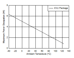
Power Dissipation Versus Ambient Temperature

Figure 8-4 is based off of a JESD51-7 4-layer, high-K board. Estimate the allowable power dissipation with the following equation. Improve thermal dissipation in the JEDEC high-K layout by adding top layer copper and increasing the number of thermal vias. See the An empirical analysis of the impact of board layout on LDO thermal performance application note. If a good thermal layout is used, the allowable thermal dissipation is improved by up to 50%.

Equation 4. TL720M05-Q1
TL720M05-Q1 TL720M05-Q1 Allowable Power
                    Dissipation Figure 8-4 TL720M05-Q1 Allowable Power Dissipation