ZHCSUM8I September   2008  – May 2024 TL720M05-Q1

PRODMIX  

  1.   1
  2. 特性
  3. 应用
  4. 说明
  5. Pin Configuration and Functions
  6. Specifications
    1. 5.1 Absolute Maximum Ratings
    2. 5.2 ESD Ratings
    3. 5.3 Recommended Operating Conditions
    4. 5.4 Thermal Information
    5. 5.5 Electrical Characteristics
    6. 5.6 Typical Characteristics
  7. Parameter Measurement Information
  8. Detailed Description
    1. 7.1 Overview
    2. 7.2 Functional Block Diagrams
    3. 7.3 Feature Description
      1. 7.3.1 Undervoltage Lockout
      2. 7.3.2 Thermal Shutdown
      3. 7.3.3 Current Limit
    4. 7.4 Device Functional Modes
      1. 7.4.1 Normal Operation
      2. 7.4.2 Dropout Operation
      3. 7.4.3 Disabled
  9. Application and Implementation
    1. 8.1 Application Information
      1. 8.1.1 Input and Output Capacitor Selection
        1. 8.1.1.1 Legacy Chip Capacitor Selection
        2. 8.1.1.2 New Chip Output Capacitor
        3. 8.1.1.3 New Chip Input Capacitor
      2. 8.1.2 Dropout Voltage
      3. 8.1.3 Reverse Current
      4. 8.1.4 Power Dissipation (PD)
        1. 8.1.4.1 Thermal Performance Versus Copper Area
        2. 8.1.4.2 Power Dissipation Versus Ambient Temperature
      5. 8.1.5 Estimating Junction Temperature
    2. 8.2 Typical Application
      1. 8.2.1 Design Requirements
      2. 8.2.2 Detailed Design Procedure
        1. 8.2.2.1 Input Capacitor
        2. 8.2.2.2 Output Capacitor
      3. 8.2.3 Application Curves
    3. 8.3 Power Supply Recommendations
    4. 8.4 Layout
      1. 8.4.1 Layout Guidelines
      2. 8.4.2 Layout Examples
  10. Device and Documentation Support
    1. 9.1 Device Support
      1. 9.1.1 Evaluation Module
      2. 9.1.2 Device Nomenclature
      3. 9.1.3 Development Support
    2. 9.2 Documentation Support
      1. 9.2.1 Related Documentation
    3. 9.3 接收文档更新通知
    4. 9.4 支持资源
    5. 9.5 Trademarks
    6. 9.6 静电放电警告
    7. 9.7 术语表
  11. 10Revision History
  12. 11Mechanical, Packaging, and Orderable Information

封装选项

请参考 PDF 数据表获取器件具体的封装图。

机械数据 (封装 | 引脚)
  • KVU|3
  • PWP|20
  • KTT|3
散热焊盘机械数据 (封装 | 引脚)
订购信息

Typical Characteristics

specified for new chip at TJ = –40°C to +150°C, VIN = 13.5V , IOUT = 100μA, COUT = 2.2µF, 1mΩ < COUT ESR < 2Ω, and CIN = 1µF (unless otherwise noted)
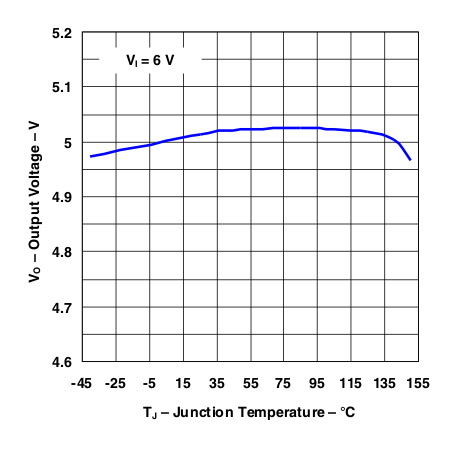
TL720M05-Q1 Output Voltage vs Junction Temperature (Legacy Chip)
 
Figure 5-1 Output Voltage vs Junction Temperature
(Legacy Chip)
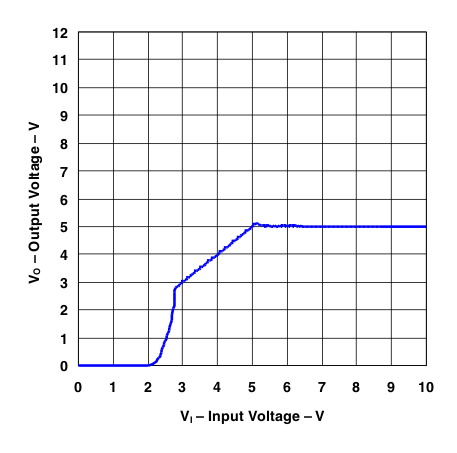
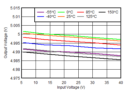
TL720M05-Q1 Output Voltage vs Input Voltage (Legacy Chip)
 
Figure 5-3 Output Voltage vs Input Voltage (Legacy Chip)
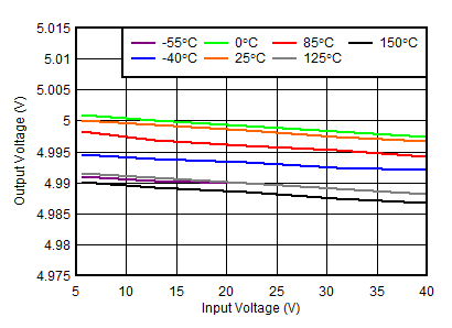
TL720M05-Q1 Line Regulation vs
                            VIN (New Chip)
VOUT = 5V, IOUT = 150mA
Figure 5-5 Line Regulation vs VIN (New Chip)
TL720M05-Q1 Line
                        Regulation vs VIN (New Chip)
VOUT = 5V, IOUT = 1mA
Figure 5-7 Line Regulation vs VIN (New Chip)
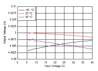
TL720M05-Q1 Line Regulation at 50mA
                        (New Chip)
COUT = 10µF, VOUT = 5V
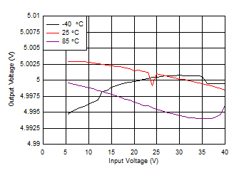
Figure 5-9 Line Regulation at 50mA (New Chip)
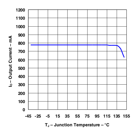
TL720M05-Q1 Output Current vs Junction Temperature (Legacy Chip)
 
Figure 5-11 Output Current vs Junction Temperature
(Legacy Chip)
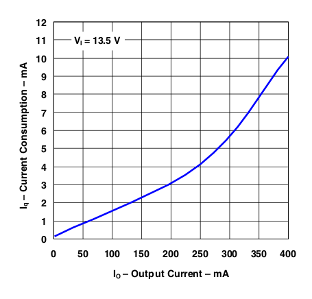
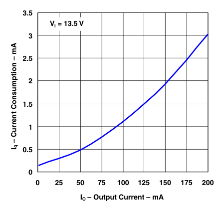
TL720M05-Q1 Current Consumption vs Output Current (Legacy
                        Chip)
 
Figure 5-13 Current Consumption vs Output Current
(Legacy Chip)
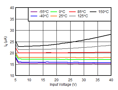
TL720M05-Q1 Quiescent Current
                            (IQ) vs VIN (New Chip)
VOUT = 5V
Figure 5-15 Quiescent Current (IQ) vs VIN (New Chip)
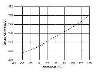
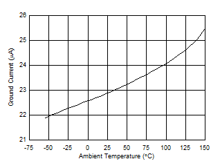
TL720M05-Q1 Ground Current at 100mA
                        (New Chip)
 
Figure 5-17 Ground Current at 100mA (New Chip)
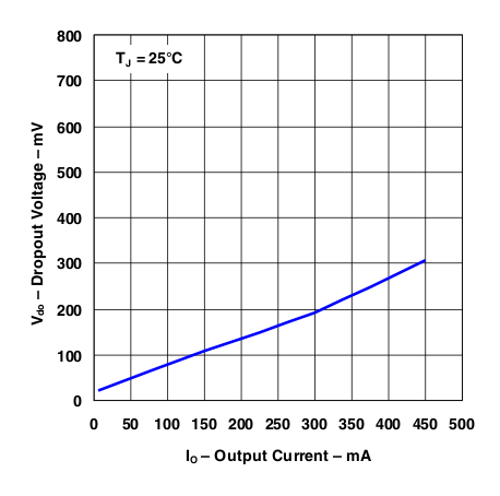
TL720M05-Q1 Dropout Voltage vs Output Current (Legacy Chip)
 
Figure 5-19 Dropout Voltage vs Output Current (Legacy Chip)
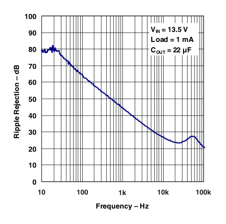
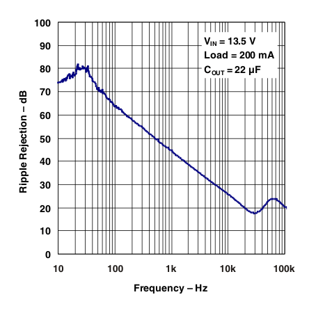
TL720M05-Q1 Power-Supply Ripple Rejection vs Frequency (Legacy Chip)
 
Figure 5-21 Power-Supply Ripple Rejection vs Frequency (Legacy Chip)
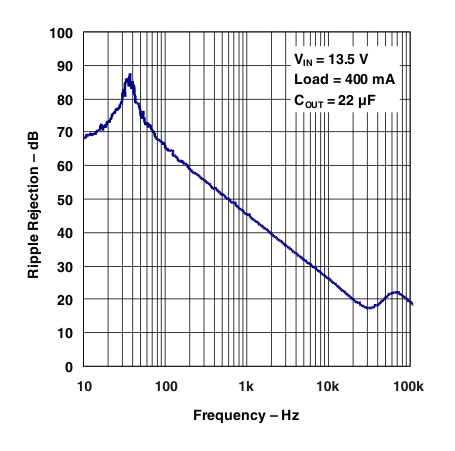
TL720M05-Q1 Power-Supply Ripple Rejection vs Frequency (Legacy Chip)
 
Figure 5-23 Power-Supply Ripple Rejection vs Frequency (Legacy Chip)
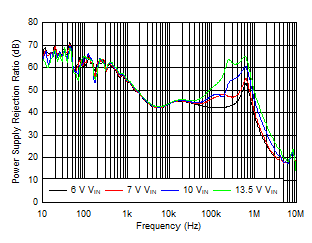
TL720M05-Q1 Power-Supply Ripple
                        Rejection vs Frequency and VIN (New Chip)
COUT = 10µF (X7R 50V), IOUT = 500mA, VOUT = 5V
Figure 5-25 Power-Supply Ripple Rejection vs Frequency and VIN (New Chip)
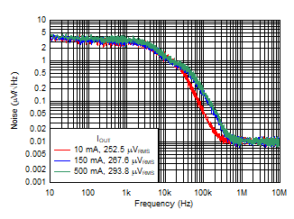
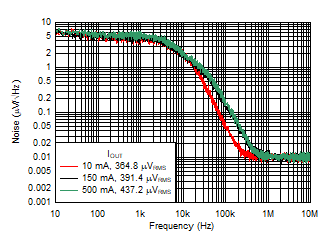
TL720M05-Q1 Noise vs Frequency (Legacy
                        Chip)
COUT = 10µF (X7R 50V), VOUT = 3.3V
 
Figure 5-27 Noise vs Frequency (Legacy Chip)
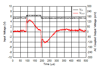
TL720M05-Q1 Line Transients (New
                        Chip)
VOUT = 5V, IOUT = 100mA, VIN = 5.5V to 6.5V,
rise time = 1µs
Figure 5-29 Line Transients (New Chip)
TL720M05-Q1 Load
                        Transient, No Load to 100mA Rising Edge (New Chip)
VOUT = 5V, IOUT = 0mA to 100mA, slew rate = 1A/µs,
COUT = 10µF
Figure 5-31 Load Transient, No Load to 100mA Rising Edge (New Chip)
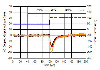
TL720M05-Q1 Load
                        Transient, 45mA to 105mA Rising Edge (New
                        Chip)
VOUT = 5V, IOUT = 45mA to 105mA, slew rate = 0.1A/µs,
COUT = 10µF
Figure 5-33 Load Transient, 45mA to 105mA Rising Edge
(New Chip)
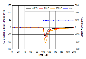
TL720M05-Q1 Load
                        Transient, No Load to 150mA Rising Edge (New Chip)
VOUT = 5V, IOUT = 0mA to 150mA, slew rate = 1A/µs,
COUT = 10µF
Figure 5-35 Load Transient, No Load to 150mA Rising Edge (New Chip)
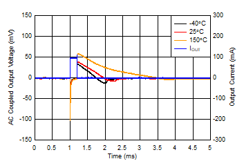
TL720M05-Q1 Load
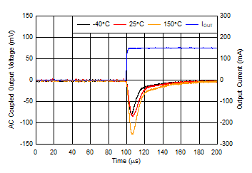
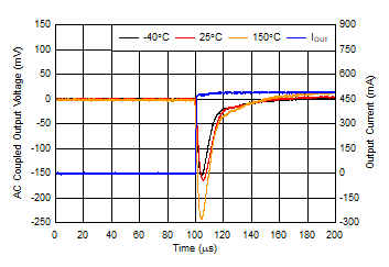
                        Transient, No Load to 500mA (New Chip)
VOUT = 5V, IOUT = 0mA to 500mA, slew rate = 1A/µs,
COUT = 10µF
Figure 5-37 Load Transient, No Load to 500mA
(New Chip)
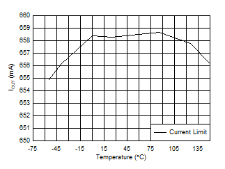
TL720M05-Q1 Output Current Limit vs
                        Temperature (New Chip)
VIN = VOUT + 1V, VOUT = 90% × VOUT(NOM)
Figure 5-39 Output Current Limit vs Temperature (New Chip)
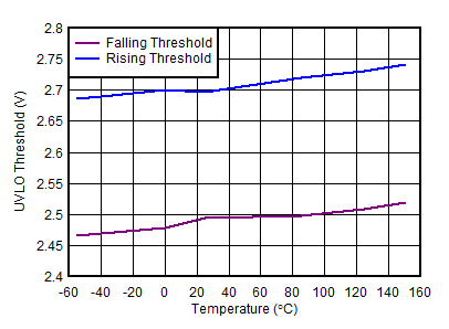
TL720M05-Q1 Undervoltage Lockout
                        (UVLO) Threshold vs Temperature (New Chip)
 
Figure 5-41 Undervoltage Lockout (UVLO) Threshold vs Temperature (New Chip)
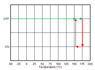
TL720M05-Q1 Thermal Shutdown (New
                        Chip)
 
Figure 5-43 Thermal Shutdown (New Chip)
TL720M05-Q1 ESR
                        Stability vs Load Capacitance (Legacy Chip)
 
Figure 5-45 ESR Stability vs Load Capacitance (Legacy Chip)
TL720M05-Q1 Output Voltage vs Junction Temperature (Legacy Chip)
 
Figure 5-2 Output Voltage vs Junction Temperature
(Legacy Chip)
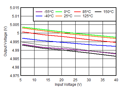
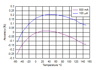
TL720M05-Q1 Output Accuracy vs
                        Temperature (New Chip)
 
Figure 5-4 Output Accuracy vs Temperature (New Chip)
TL720M05-Q1 Line
                        Regulation vs VIN (New Chip)
VOUT = 5V, IOUT = 5mA
Figure 5-6 Line Regulation vs VIN (New Chip)
TL720M05-Q1 Load Regulation vs
                            IOUT (New Chip)
VOUT = 5V
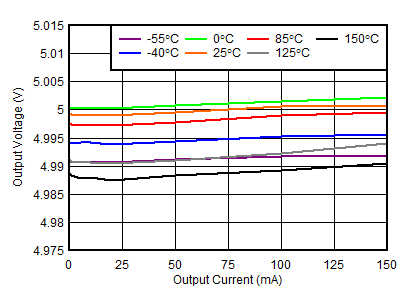
Figure 5-8 Load Regulation vs IOUT (New Chip)
TL720M05-Q1 Line Regulation at 100mA
                        (New Chip)
COUT = 10µF, VOUT = 5V
Figure 5-10 Line Regulation at 100mA (New Chip)
TL720M05-Q1 Current Consumption vs Output Current (Legacy
                        Chip)
 
Figure 5-12 Current Consumption vs Output Current
(Legacy Chip)
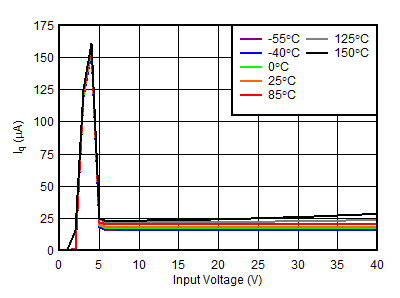
TL720M05-Q1 Quiescent Current
                            (IQ) vs VIN
                        (New Chip)
 
Figure 5-14 Quiescent Current (IQ) vs VIN
(New Chip)
TL720M05-Q1 Ground Current
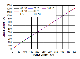
                            (IGND) vs IOUT (New Chip)
 
Figure 5-16 Ground Current (IGND) vs IOUT (New Chip)
TL720M05-Q1 Ground Current at 500µA
                        (New Chip)
 
Figure 5-18 Ground Current at 500µA (New Chip)
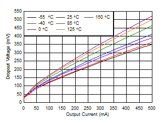
TL720M05-Q1 Dropout Voltage
                            (VDO) vs IOUT (New Chip)
VIN = 3V
Figure 5-20 Dropout Voltage (VDO) vs IOUT (New Chip)
TL720M05-Q1 Power-Supply Ripple Rejection vs Frequency (Legacy Chip)
 
Figure 5-22 Power-Supply Ripple Rejection vs Frequency (Legacy Chip)
TL720M05-Q1 Power-Supply Ripple
                        Rejection vs Frequency and IOUT (New Chip)
COUT = 10µF (X7R 50V), VOUT = 5V
Figure 5-24 Power-Supply Ripple Rejection vs Frequency and IOUT (New Chip)
TL720M05-Q1 Noise vs Frequency (Legacy
                        Chip)
COUT = 10µF (X7R 50V), VOUT = 5V
Figure 5-26 Noise vs Frequency (Legacy Chip)
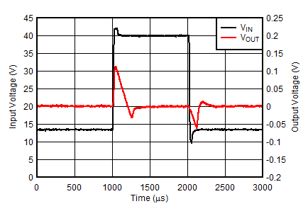
TL720M05-Q1 Line Transients (New
                        Chip)
VOUT = 5V, IOUT = 1mA, VIN = 13.5V to 45V,
slew rate = 2.7V/µs
Figure 5-28 Line Transients (New Chip)
TL720M05-Q1 Load Transient, No Load to
                        100mA (New Chip)
VOUT = 5V, IOUT = 0mA to 100mA, slew rate = 1A/µs,
COUT = 10µF
Figure 5-30 Load Transient, No Load to 100mA (New Chip)
TL720M05-Q1 Load Transient, 45mA to
                        105mA (New Chip)
VOUT = 5V, IOUT = 45mA to 105mA, slew rate = 0.1A/µs,
COUT = 10µF
Figure 5-32 Load Transient, 45mA to 105mA
(New Chip)
TL720M05-Q1 Load
                        Transient, No Load to 150mA (New Chip)
VOUT = 5V, IOUT = 0mA to 150mA, slew rate = 1A/µs,
COUT = 10µF
Figure 5-34 Load Transient, No Load to 150mA
(New Chip)
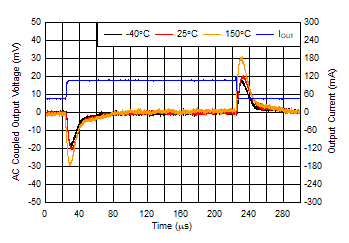
TL720M05-Q1 Load
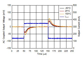
                        Transient, 150mA to 350mA (New Chip)
VOUT = 5V, IOUT = 150mA to 350mA, slew rate = 0.1A/µs, COUT = 10µF
Figure 5-36 Load Transient, 150mA to 350mA
(New Chip)
TL720M05-Q1 Load
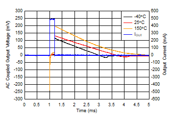
                        Transient, No Load to 500mA Rising Edge (New Chip)
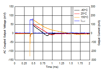
VOUT = 5V, IOUT = 0mA to 500mA, slew rate = 1A/µs,
COUT = 10µF
Figure 5-38 Load Transient, No Load to 500mA Rising Edge (New Chip)
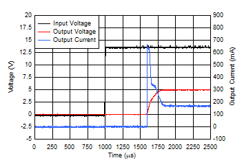
TL720M05-Q1 Start-Up Plot Inrush
                        Current (New Chip)
VIN = VOUT + 1V, VOUT = 90% × VOUT(NOM)
Figure 5-40 Start-Up Plot Inrush Current (New Chip)
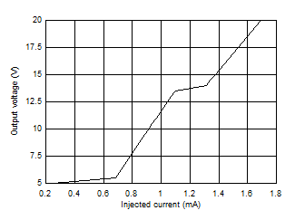
TL720M05-Q1 Output Voltage vs Injected
                        Current (New Chip)
 
Figure 5-42 Output Voltage vs Injected Current
(New Chip)
TL720M05-Q1 ESR
                        Stability vs Load Current (Legacy Chip)
 
Figure 5-44 ESR Stability vs Load Current (Legacy Chip)
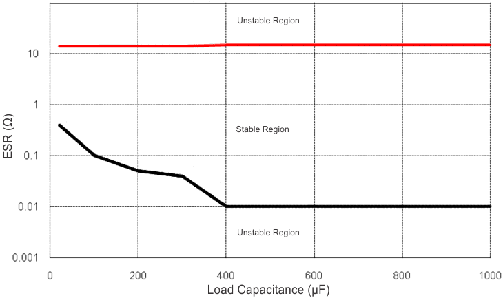
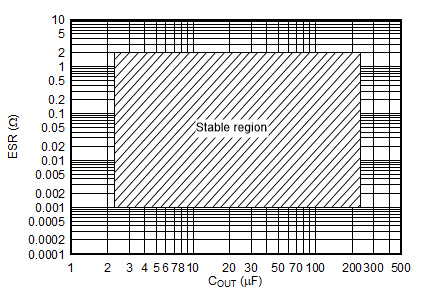
TL720M05-Q1 Stability, ESR vs
                            COUT (New Chip)
 
Figure 5-46 Stability, ESR vs COUT (New Chip)