ZHCSUM8I September 2008 – May 2024 TL720M05-Q1
PRODMIX
- 1
- 1 特性
- 2 应用
- 3 说明
- 4 Pin Configuration and Functions
- 5 Specifications
- 6 Parameter Measurement Information
- 7 Detailed Description
- 8 Application and Implementation
- 9 Device and Documentation Support
- 10Revision History
- 11Mechanical, Packaging, and Orderable Information
封装选项
请参考 PDF 数据表获取器件具体的封装图。
机械数据 (封装 | 引脚)
- KVU|3
- PWP|20
- KTT|3
散热焊盘机械数据 (封装 | 引脚)
订购信息
8.1.4.1 Thermal Performance Versus Copper Area
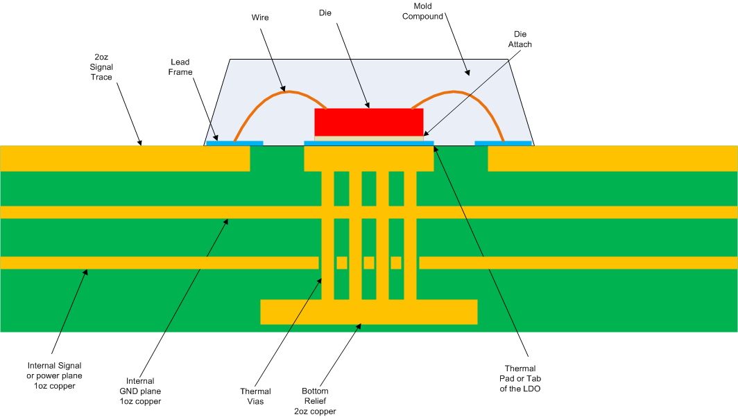
The most used thermal resistance parameter RθJA is highly dependent on the heat-spreading capability built into the particular PCB design. Therefore, RθJA varies according to the total copper area, copper weight, and location of the planes. The RθJA recorded in the Thermal Information table is determined by the JEDEC standard (see Figure 8-1), PCB, and copper-spreading area. RθJA is only used as a relative measure of package thermal performance. For a well-designed thermal layout, RθJA is actually the sum of RθJCbot plus the thermal resistance contribution by the PCB copper. RθJCbot is the package junction-to-case (bottom) thermal resistance.
 Figure 8-1 JEDEC Standard 2s2p PCB
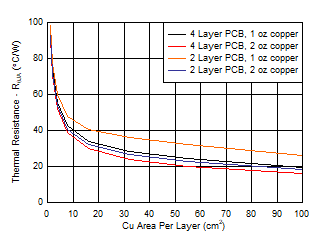
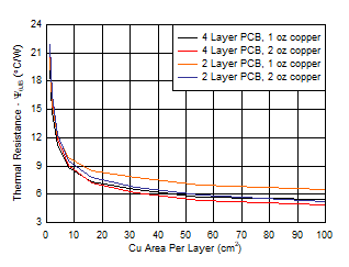
Figure 8-2 and Figure 8-3 show the functions of RθJA and ψJB versus copper area and thickness. These plots are generated with a 101.6mm × 101.6mm × 1.6mm PCB of two and four layers. For the 4-layer board, inner planes use 1oz copper thickness. Outer layers are simulated with both 1oz and 2oz copper thickness. A 3×4 (KVU package) array of thermal vias with a 300µm drill diameter and 25µm copper plating is located beneath the device thermal pad. The thermal vias connect the top layer, the bottom layer and, in the case of the 4-layer board, the first inner GND plane. Each of the layers has a copper plane of equal area.
 Figure 8-2 RθJA vs Copper
Area (KVU Package)
 Figure 8-3 ψJB vs Copper
Area (KVU Package)