SLVS220G July 1999 – August 2016 TL7700
PRODUCTION DATA.
- 1 Features
- 2 Applications
- 3 Description
- 4 Revision History
- 5 Pin Configuration and Functions
- 6 Specifications
- 7 Parameter Measurement Information
- 8 Detailed Description
- 9 Application and Implementation
- 10Power Supply Recommendations
- 11Layout
- 12Device and Documentation Support
- 13Mechanical, Packaging, and Orderable Information
封装选项
机械数据 (封装 | 引脚)
散热焊盘机械数据 (封装 | 引脚)
- PS|8
订购信息
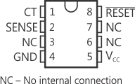
5 Pin Configuration and Functions
DGK Package
8-Pin VSSOP
Top View

P, PS, or PW Package
8-Pin PDIP, SO, TSSOP
Top View

Pin Functions
| PIN | I/O | DESCRIPTION | ||
|---|---|---|---|---|
| NAME | PDIP, SO, TSSOP |
VSSOP | ||
| CT | 1 | 3 | I/O | Timing capacitor connection. This terminal sets the RESET output pulse duration (tpo). It is connected internally to a 15-µA constant-current source. There is a limit on the switching speed of internal elements; even if CT is set to 0, response speeds remain at approximately 5 to 10 µs. If CT is open, the device can be used as an adjustable-threshold noninverting comparator. If CT is low, the internal output-stage comparator is active, and the RESET output transistor is on. An external voltage must not be applied to this terminal due to the internal structure of the device. Therefore, drive the device using an open-collector transistor, FET, or 3-state buffer (in the low-level or high-impedance state). |
| GND | 4 | 5 | — | Ground Keep this terminal as low impedance as possible to reduce circuit noise. |
| NC | 3, 6, 7 | 2, 6, 7 | — | No internal connection |
| RESET | 8 | 1 | O | Reset output This terminal can be connected directly to a system that resets in the active-low state. A pullup resistor usually is required because the output is an npn open-collector transistor. An additional transistor should be connected when the active-high reset or higher output current is required. |
| SENSE | 2 | 4 | I | Voltage sense This terminal has a threshold level of 500 mV. The sense voltage and hysteresis can be set at the same time when the two voltage-dividing resistors are connected. The reference voltage is temperature compensated to inhibit temperature drift in the threshold voltage within the operating temperature range. |
| VCC | 5 | 8 | — | Power supply This terminal is used in an operating-voltage range of 1.8 V to 40 V. |