SLVS028K April 1983 – September 2016 TL7702A , TL7705A , TL7709A , TL7712A , TL7715A
PRODUCTION DATA.
- 1 Features
- 2 Applications
- 3 Description
- 4 Revision History
- 5 Pin Configuration and Functions
- 6 Specifications
- 7 Parameter Measurement Information
- 8 Detailed Description
- 9 Application and Implementation
- 10Power Supply Recommendations
- 11Layout
- 12Device and Documentation Support
- 13Mechanical, Packaging, and Orderable Information
8 Detailed Description
8.1 Overview
The TL77xxA family of integrated-circuit supply-voltage supervisors is designed specifically for use as reset controllers in microcomputer and microprocessor systems. The supply-voltage supervisor monitors the supply for undervoltage conditions at the SENSE input. During power up, the RESET output becomes active (low) when VCC attains a value approaching 3.6 V. At this point (assuming that SENSE is above VIT+), the delay timer function activates a time delay, after which outputs RESET and RESET go inactive (high and low, respectively). When an undervoltage condition occurs during normal operation, RESET and RESET go active. To ensure that a complete reset occurs, the reset outputs remain active for a time delay after the voltage at the SENSE input exceeds the positive-going threshold value.
During power down and when SENSE is below VIT−, the outputs remain active until VCC falls below 2 V. After this, the outputs are undefined. An external capacitor (typically 0.1 μF) must be connected to REF to reduce the influence of fast transients in the supply voltage.
Five versions of this circuit are available:
- TL7705A (Vt = 4.55 V): Application in TTL-systems and microcomputer systems which require a 5 volt supply (for example, TMS7000)
- TL7709A (Vt = 7.6 V): Application in microcomputer systems using the TMS1XXXNLL
- TL7712A (Vt = 10.8 V): Application in CMOS, microprocessor, and memory circuits with a 12 volt supply.
- TL7715A (Vt = 13.5 V): Application in circuits which operate with a supply voltage of 15 V, as is found often in analog circuits.
- TL7702A (Vt = 2.5 V): Application in systems where other supply voltages are used. The required trigger level my be adjusted with an external resistor divider at the SENSE input.
8.2 Functional Block Diagram
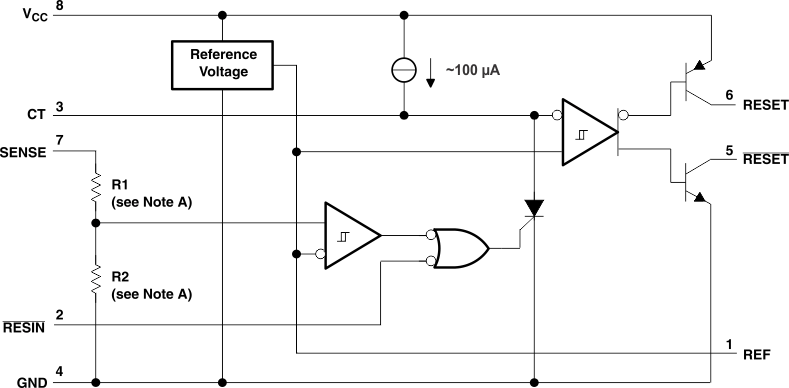
The functional block diagram is shown for illustrative purposes only; the actual circuit includes a trimming network to adjust the reference voltage and sense-comparator trip point.

8.3 Feature Description
8.3.1 Wide Supply-Voltage Range
Th TL77xxA family operates of a wide supply voltage range of 3.5 V to 18 V.
8.3.2 Externally Adjustable Pulse Duration
The time delay is determined by the value of the external capacitor CT: td = 1.3 × 10⁴ × CT, where CT is in farads (F) and td is in seconds (s).
8.3.3 Temperature-Compensated Voltage Reference
The series TL77xxA incorporates an extremely stable reference voltage source. This voltage source can also be used in applications where a constant voltage source is required. The reference voltage varies less than 10 mV over the supply voltage range of 3.5 V to 18 V. The same stability of the reference voltage is maintained, when the ambient temperature is changed. The reference's voltage varies only 16 mV when the ambient temperature is changed from –40°C to +85°C.
8.4 Device Functional Modes
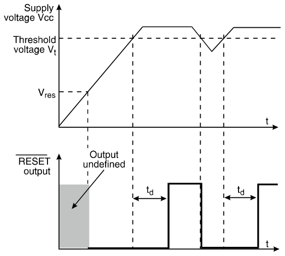
Figure 7 shows the timing of the various signals. In this example the SENSE input is connected to the supply voltage VCC as in typical applications of this device. The minimum supply voltage for which the function of this device is guaranteed is 3.6 V. After power-on, the outputs are undefined until the minimum supply voltage Vres is reached. For the TL77xxA the minimum supply voltage is Vres = 3 V (typical 2.5 V). Beyond the voltage Vres the capacitor CT is first kept discharged, and the outputs stay in the active state (RESET = High, RESET = Low). When the input voltage becomes higher than the threshold voltage Vt, the thyristor is turned off and the capacitor is charged. After a delay, td, the voltage at the capacitor passes the trigger level of the output comparator and the outputs become inactive. The circuit to be initialized is now set to a defined state and starts the correct operation.
