ZHCSH32 November   2017 TLA2021 , TLA2022 , TLA2024

PRODUCTION DATA.  

  1. 特性
  2. 应用
  3. 说明
    1.     Device Images
      1.      系统监控应用示例
  4. 修订历史记录
  5. Device Comparison Table
  6. Pin Configuration and Functions
    1.     Pin Functions
  7. Specifications
    1. 7.1 Absolute Maximum Ratings
    2. 7.2 ESD Ratings
    3. 7.3 Recommended Operating Conditions
    4. 7.4 Thermal Information
    5. 7.5 Electrical Characteristics
    6. 7.6 I2C Timing Requirements
    7. 7.7 Typical Characteristics
  8. Detailed Description
    1. 8.1 Overview
    2. 8.2 Functional Block Diagrams
    3. 8.3 Feature Description
      1. 8.3.1 Multiplexer
      2. 8.3.2 Analog Inputs
      3. 8.3.3 Full-Scale Range (FSR) and LSB Size
      4. 8.3.4 Voltage Reference
      5. 8.3.5 Oscillator
      6. 8.3.6 Output Data Rate and Conversion Time
    4. 8.4 Device Functional Modes
      1. 8.4.1 Reset and Power-Up
      2. 8.4.2 Operating Modes
        1. 8.4.2.1 Single-Shot Conversion Mode
        2. 8.4.2.2 Continuous-Conversion Mode
    5. 8.5 Programming
      1. 8.5.1 I2C Interface
        1. 8.5.1.1 I2C Address Selection
        2. 8.5.1.2 I2C Interface Speed
        3. 8.5.1.3 Serial Clock (SCL) and Serial Data (SDA)
        4. 8.5.1.4 I2C Data Transfer Protocol
        5. 8.5.1.5 Timeout
        6. 8.5.1.6 I2C General-Call (Software Reset)
      2. 8.5.2 Reading and Writing Register Data
        1. 8.5.2.1 Reading Conversion Data or the Configuration Register
        2. 8.5.2.2 Writing the Configuration Register
      3. 8.5.3 Data Format
  9. Register Maps
    1. 9.1 Conversion Data Register (RP = 00h) [reset = 0000h]
      1. Table 6. Conversion Data Register Field Descriptions
    2. 9.2 Configuration Register (RP = 01h) [reset = 8583h]
      1. Table 7. Configuration Register Field Descriptions
  10. 10Application and Implementation
    1. 10.1 Application Information
      1. 10.1.1 Basic Interface Connections
      2. 10.1.2 Connecting Multiple Devices
      3. 10.1.3 Single-Ended Signal Measurements
      4. 10.1.4 Analog Input Filtering
      5. 10.1.5 Duty Cycling To Reduce Power Consumption
      6. 10.1.6 I2C Communication Sequence Example
    2. 10.2 Typical Application
      1. 10.2.1 Design Requirements
      2. 10.2.2 Detailed Design Procedure
      3. 10.2.3 Application Curve
  11. 11Power Supply Recommendations
    1. 11.1 Power-Supply Sequencing
    2. 11.2 Power-Supply Decoupling
  12. 12Layout
    1. 12.1 Layout Guidelines
    2. 12.2 Layout Example
  13. 13器件和文档支持
    1. 13.1 器件支持
      1. 13.1.1 Third-Party Products Disclaimer
    2. 13.2 相关链接
    3. 13.3 接收文档更新通知
    4. 13.4 社区资源
    5. 13.5 商标
    6. 13.6 静电放电警告
    7. 13.7 Glossary
  14. 14机械、封装和可订购信息

封装选项

机械数据 (封装 | 引脚)
散热焊盘机械数据 (封装 | 引脚)
订购信息

Connecting Multiple Devices

Up to three TLA202x devices can be connected to a single I2C bus by using different address pin configurations for each device. Use the address pin to set the TLA202x to one of three different I2C addresses. Figure 19 shows an example with three TLA202x devices on the same I2C bus. One set of pullup resistors is required per bus line. The pullup resistor values may need to decrease to compensate for the additional bus capacitance presented by multiple devices and increased line length.
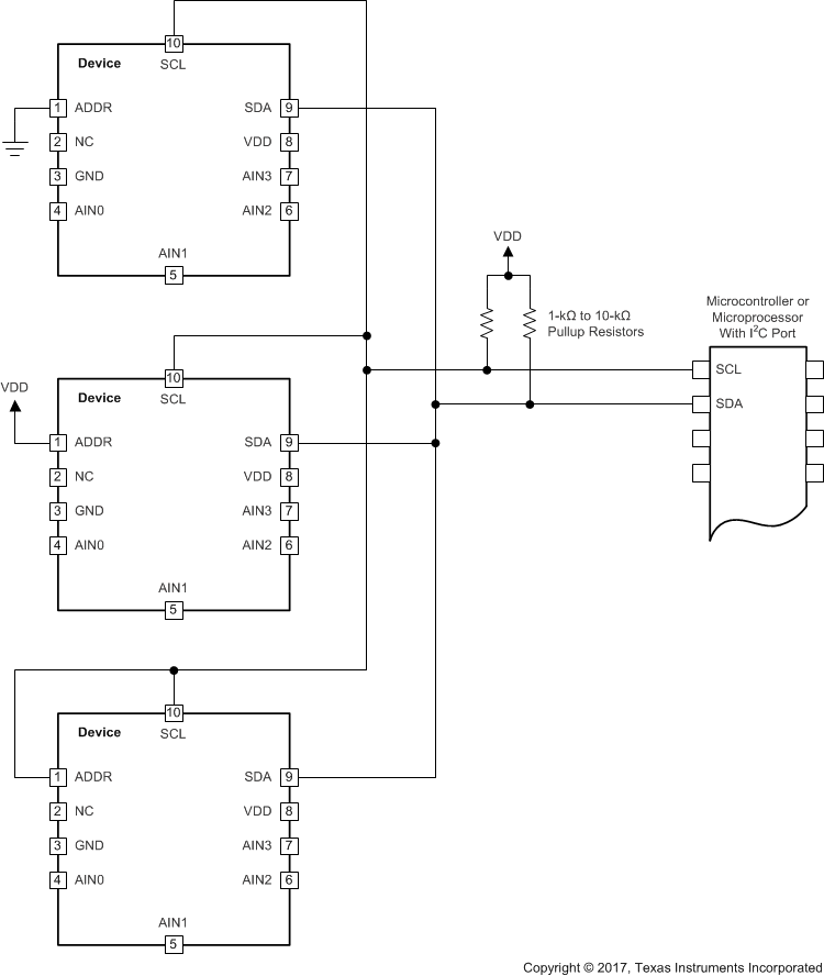
TLA2021 TLA2022 TLA2024 ai_multi_device_connection_bas822.gif

NOTE:

The TLA202x power and input connections are omitted for clarity. The ADDR pin selects the I2C address.
Figure 19. Connecting Multiple TLA202x Devices