ZHCSH32 November   2017 TLA2021 , TLA2022 , TLA2024

PRODUCTION DATA.  

  1. 特性
  2. 应用
  3. 说明
    1.     Device Images
      1.      系统监控应用示例
  4. 修订历史记录
  5. Device Comparison Table
  6. Pin Configuration and Functions
    1.     Pin Functions
  7. Specifications
    1. 7.1 Absolute Maximum Ratings
    2. 7.2 ESD Ratings
    3. 7.3 Recommended Operating Conditions
    4. 7.4 Thermal Information
    5. 7.5 Electrical Characteristics
    6. 7.6 I2C Timing Requirements
    7. 7.7 Typical Characteristics
  8. Detailed Description
    1. 8.1 Overview
    2. 8.2 Functional Block Diagrams
    3. 8.3 Feature Description
      1. 8.3.1 Multiplexer
      2. 8.3.2 Analog Inputs
      3. 8.3.3 Full-Scale Range (FSR) and LSB Size
      4. 8.3.4 Voltage Reference
      5. 8.3.5 Oscillator
      6. 8.3.6 Output Data Rate and Conversion Time
    4. 8.4 Device Functional Modes
      1. 8.4.1 Reset and Power-Up
      2. 8.4.2 Operating Modes
        1. 8.4.2.1 Single-Shot Conversion Mode
        2. 8.4.2.2 Continuous-Conversion Mode
    5. 8.5 Programming
      1. 8.5.1 I2C Interface
        1. 8.5.1.1 I2C Address Selection
        2. 8.5.1.2 I2C Interface Speed
        3. 8.5.1.3 Serial Clock (SCL) and Serial Data (SDA)
        4. 8.5.1.4 I2C Data Transfer Protocol
        5. 8.5.1.5 Timeout
        6. 8.5.1.6 I2C General-Call (Software Reset)
      2. 8.5.2 Reading and Writing Register Data
        1. 8.5.2.1 Reading Conversion Data or the Configuration Register
        2. 8.5.2.2 Writing the Configuration Register
      3. 8.5.3 Data Format
  9. Register Maps
    1. 9.1 Conversion Data Register (RP = 00h) [reset = 0000h]
      1. Table 6. Conversion Data Register Field Descriptions
    2. 9.2 Configuration Register (RP = 01h) [reset = 8583h]
      1. Table 7. Configuration Register Field Descriptions
  10. 10Application and Implementation
    1. 10.1 Application Information
      1. 10.1.1 Basic Interface Connections
      2. 10.1.2 Connecting Multiple Devices
      3. 10.1.3 Single-Ended Signal Measurements
      4. 10.1.4 Analog Input Filtering
      5. 10.1.5 Duty Cycling To Reduce Power Consumption
      6. 10.1.6 I2C Communication Sequence Example
    2. 10.2 Typical Application
      1. 10.2.1 Design Requirements
      2. 10.2.2 Detailed Design Procedure
      3. 10.2.3 Application Curve
  11. 11Power Supply Recommendations
    1. 11.1 Power-Supply Sequencing
    2. 11.2 Power-Supply Decoupling
  12. 12Layout
    1. 12.1 Layout Guidelines
    2. 12.2 Layout Example
  13. 13器件和文档支持
    1. 13.1 器件支持
      1. 13.1.1 Third-Party Products Disclaimer
    2. 13.2 相关链接
    3. 13.3 接收文档更新通知
    4. 13.4 社区资源
    5. 13.5 商标
    6. 13.6 静电放电警告
    7. 13.7 Glossary
  14. 14机械、封装和可订购信息

封装选项

机械数据 (封装 | 引脚)
散热焊盘机械数据 (封装 | 引脚)
订购信息

Single-Ended Signal Measurements

The TLA2021 and TLA2022 can measure one single-ended signal, and the TLA2024 up to four single-ended signals. To measure single-ended signals with the TLA2021 and TLA2022, connect AIN1 to GND externally. The TLA2024 measures single-ended signals by properly configuring the MUX[2:0] bits (settings 100 to 111) in the configuration register. Figure 20 shows a single-ended connection scheme for the TLA2024 highlighted in red (a differential connection scheme is shown in green). The single-ended signal range is from 0 V up to the positive supply or +FS (whichever is lower). Negative voltages cannot be applied to these devices because the TLA202x can only accept positive voltages with respect to ground. Only the code range from 0000h to 7FF0h (or a subset thereof in case +FS > VDD) is used in this case.
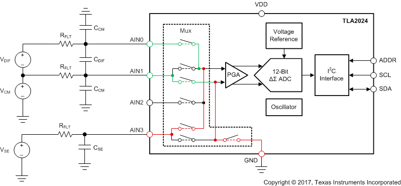
TLA2021 TLA2022 TLA2024 ai_filtering_bas846.gifFigure 20. Filter Implementation for Single-Ended and Differential Signal Measurements

The TLA2024 also allows AIN3 to serve as a common point for measurements by appropriately setting the MUX[2:0] bits. AIN0, AIN1, and AIN2 can all be measured with respect to AIN3. In this configuration, the usable voltage and code range, respectively, is increased over the single-ended configuration because negative differential voltages are allowed when GND < V(AIN3)< VDD. Assume the following settings for example: VDD = 5 V, FSR = ±2.048 V, AINP = AIN0, and AINN = AIN3 = 2.5 V. In this case, the voltage at AIN0 can swing from V(AIN0) = 2.5 V – 2.048 V to 2.5 V + 2.048 V using the entire full-scale range.