ZHCSJS9 May   2019 TLA2528

ADVANCE INFORMATION for pre-production products; subject to change without notice.  

  1. 特性
  2. 应用
  3. 说明
    1.     Device Images
      1.      TLA2528 方框图和 应用
  4. 修订历史记录
  5. Pin Configuration and Functions
    1.     Pin Functions
  6. Specifications
    1. 6.1      Absolute Maximum Ratings
    2. 6.2      ESD Ratings
    3. 6.3      Recommended Operating Conditions
    4. 6.4      Thermal Information
    5. 6.5      Electrical Characteristics
    6. Table 1. I2C Timing Requirements
    7. Table 2. Timing Requirements
    8. Table 3. I2C Switching Characteristics
    9. 6.6      Switching Characteristics
  7. Detailed Description
    1. 7.1 Overview
    2. 7.2 Functional Block Diagram
    3. 7.3 Feature Description
      1. 7.3.1  Multiplexer and ADC
      2. 7.3.2  Reference
      3. 7.3.3  ADC Transfer Function
      4. 7.3.4  ADC Offset Calibration
      5. 7.3.5  I2C Address Selector
      6. 7.3.6  Programmable Averaging Filter
      7. 7.3.7  General-Purpose I/Os (GPIOs)
      8. 7.3.8  Oscillator and Timing Control
      9. 7.3.9  Output Data Format
      10. 7.3.10 I2C Protocol Features
        1. 7.3.10.1 General Call
        2. 7.3.10.2 General Call With Software Reset
        3. 7.3.10.3 General Call With a Software Write to the Programmable Part of the Slave Address
        4. 7.3.10.4 Configuring the Device for High-Speed I2C Mode
    4. 7.4 Device Functional Modes
      1. 7.4.1 Device Power-Up and Reset
      2. 7.4.2 Manual Mode
      3. 7.4.3 Auto-Sequence Mode
    5. 7.5 Programming
      1. 7.5.1 Reading Registers
        1. 7.5.1.1 Single Register Read
        2. 7.5.1.2 Reading a Continuous Block of Registers
      2. 7.5.2 Writing Registers
        1. 7.5.2.1 Single Register Write
        2. 7.5.2.2 Set Bit
        3. 7.5.2.3 Clear Bit
        4. 7.5.2.4 Writing a Continuous Block of Registers
    6. 7.6 TLA2528 Registers
      1. 7.6.1  SYSTEM_STATUS Register (Address = 0x0) [reset = 0x80]
        1. Table 13. SYSTEM_STATUS Register Field Descriptions
      2. 7.6.2  GENERAL_CFG Register (Address = 0x1) [reset = 0x0]
        1. Table 14. GENERAL_CFG Register Field Descriptions
      3. 7.6.3  DATA_CFG Register (Address = 0x2) [reset = 0x0]
        1. Table 15. DATA_CFG Register Field Descriptions
      4. 7.6.4  OSR_CFG Register (Address = 0x3) [reset = 0x0]
        1. Table 16. OSR_CFG Register Field Descriptions
      5. 7.6.5  OPMODE_CFG Register (Address = 0x4) [reset = 0x0]
        1. Table 17. OPMODE_CFG Register Field Descriptions
      6. 7.6.6  PIN_CFG Register (Address = 0x5) [reset = 0x0]
        1. Table 18. PIN_CFG Register Field Descriptions
      7. 7.6.7  GPIO_CFG Register (Address = 0x7) [reset = 0x0]
        1. Table 19. GPIO_CFG Register Field Descriptions
      8. 7.6.8  GPO_DRIVE_CFG Register (Address = 0x9) [reset = 0x0]
        1. Table 20. GPO_DRIVE_CFG Register Field Descriptions
      9. 7.6.9  GPO_OUTPUT_VALUE Register (Address = 0xB) [reset = 0x0]
        1. Table 21. GPO_OUTPUT_VALUE Register Field Descriptions
      10. 7.6.10 GPI_VALUE_LSB Register (Address = 0xD) [reset = 0x0]
        1. Table 22. GPI_VALUE_LSB Register Field Descriptions
      11. 7.6.11 SEQUENCE_CFG Register (Address = 0x10) [reset = 0x0]
        1. Table 23. SEQUENCE_CFG Register Field Descriptions
      12. 7.6.12 CHANNEL_SEL Register (Address = 0x11) [reset = 0x0]
        1. Table 24. CHANNEL_SEL Register Field Descriptions
      13. 7.6.13 AUTO_SEQ_CHSEL Register (Address = 0x12) [reset = 0x0]
        1. Table 25. AUTO_SEQ_CHSEL Register Field Descriptions
  8. Application and Implementation
    1. 8.1 Application Information
    2. 8.2 Typical Applications
      1. 8.2.1 Mixed-Channel Configuration
        1. 8.2.1.1 Design Requirements
        2. 8.2.1.2 Detailed Design Procedure
          1. 8.2.1.2.1 Digital Input
          2. 8.2.1.2.2 Digital Open-Drain Output
        3. 8.2.1.3 Digital Push-Pull Output
  9. Power Supply Recommendations
    1. 9.1 AVDD and DVDD Supply Recommendations
  10. 10Layout
    1. 10.1 Layout Guidelines
    2. 10.2 Layout Example
  11. 11器件和文档支持
    1. 11.1 接收文档更新通知
    2. 11.2 社区资源
    3. 11.3 商标
    4. 11.4 静电放电警告
    5. 11.5 Glossary
  12. 12机械、封装和可订购信息

封装选项

机械数据 (封装 | 引脚)
散热焊盘机械数据 (封装 | 引脚)
订购信息

Multiplexer and ADC

The eight channels of the multiplexer can be independently configured as ADC inputs or general-purpose inputs/outputs (GPIOs). Figure 2 shows that each input pin has electrostatic discharge (ESD) protection diodes to AVDD and GND. On power-up or after device reset, all eight multiplexer channels are configured as analog inputs.

Figure 2 shows an equivalent circuit for pins configured as analog inputs. The ADC sampling switch is represented by an ideal switch (SW) in series with the resistor, RSW (typically 150 Ω), and the sampling capacitor, CSH (typically 12 pF).
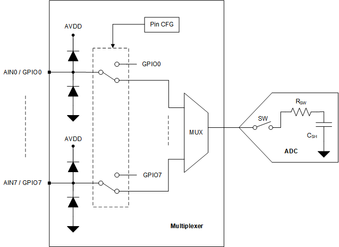
TLA2528 mux_structure.gifFigure 2. Analog Inputs, GPIOs, and ADC Connections

During acquisition, the SW switch is closed to allow the signal on the selected analog input channel to charge the internal sampling capacitor. During conversion, the SW switch is opened to disconnect the analog input channel from the sampling capacitor.

The multiplexer channels can be configured as GPIOs in the PIN_CFG register. The direction of a GPIO (either as an input or an output) can be set in the GPIO_CFG register. The logic level on the channels configured as digital inputs can be read from the GPI_VALUE register. The digital outputs can be accessed by writing to the GPO_OUTPUT_VALUE register. The digital outputs can be configured as either open-drain or push-pull in the GPO_DRIVE_CFG register.