ZHCSJS9 May 2019 TLA2528
ADVANCE INFORMATION for pre-production products; subject to change without notice.
- 1 特性
- 2 应用
- 3 说明
- 4 修订历史记录
- 5 Pin Configuration and Functions
- 6 Specifications
-
7 Detailed Description
- 7.1 Overview
- 7.2 Functional Block Diagram
- 7.3 Feature Description
- 7.4 Device Functional Modes
- 7.5 Programming
- 7.6
TLA2528 Registers
- 7.6.1 SYSTEM_STATUS Register (Address = 0x0) [reset = 0x80]
- 7.6.2 GENERAL_CFG Register (Address = 0x1) [reset = 0x0]
- 7.6.3 DATA_CFG Register (Address = 0x2) [reset = 0x0]
- 7.6.4 OSR_CFG Register (Address = 0x3) [reset = 0x0]
- 7.6.5 OPMODE_CFG Register (Address = 0x4) [reset = 0x0]
- 7.6.6 PIN_CFG Register (Address = 0x5) [reset = 0x0]
- 7.6.7 GPIO_CFG Register (Address = 0x7) [reset = 0x0]
- 7.6.8 GPO_DRIVE_CFG Register (Address = 0x9) [reset = 0x0]
- 7.6.9 GPO_OUTPUT_VALUE Register (Address = 0xB) [reset = 0x0]
- 7.6.10 GPI_VALUE_LSB Register (Address = 0xD) [reset = 0x0]
- 7.6.11 SEQUENCE_CFG Register (Address = 0x10) [reset = 0x0]
- 7.6.12 CHANNEL_SEL Register (Address = 0x11) [reset = 0x0]
- 7.6.13 AUTO_SEQ_CHSEL Register (Address = 0x12) [reset = 0x0]
- 8 Application and Implementation
- 9 Power Supply Recommendations
- 10Layout
- 11器件和文档支持
- 12机械、封装和可订购信息
7.3.3 ADC Transfer Function
The ADC output is in straight binary format. Equation 1 computes the ADC resolution:
Equation 1. 1 LSB = VREF / 2N
where
- VREF = AVDD
- N = 12
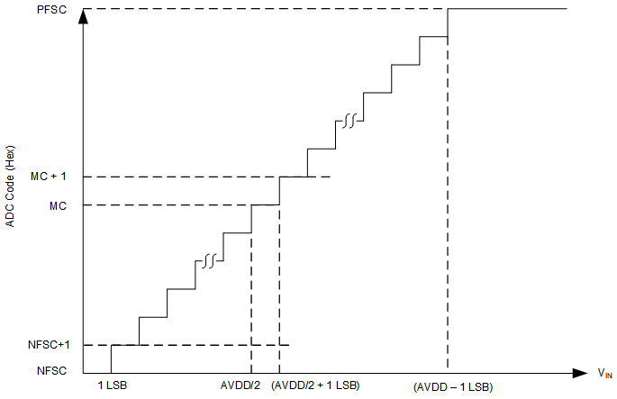
Figure 3 and Table 4 detail the transfer characteristics for the device.
 Figure 3. Ideal Transfer Characteristics
 Table 4. Transfer Characteristics
| INPUT VOLTAGE | CODE | DESCRIPTION | IDEAL OUTPUT CODE |
|---|---|---|---|
| ≤1 LSB | NFSC | Negative full-scale code | 000 |
| 1 LSB to 2 LSBs | NFSC + 1 | — | 001 |
| (AVDD / 2) to (AVDD / 2) + 1 LSB | MC | Mid code | 800 |
| (AVDD / 2) + 1 LSB to (AVDD / 2) + 2 LSB | MC + 1 | — | 801 |
| ≥ AVDD – 1 LSB | PFSC | Positive full-scale code | FFF |