SLOS190H February 1997 – March 2016 TLC2272 , TLC2272A , TLC2272AM , TLC2272M , TLC2274 , TLC2274A , TLC2274AM
PRODUCTION DATA.
- 1 Features
- 2 Applications
- 3 Description
- 4 Revision History
- 5 Pin Configuration and Functions
-
6 Specifications
- 6.1 Absolute Maximum Ratings
- 6.2 ESD Ratings
- 6.3 Recommended Operating Conditions
- 6.4 Thermal Information
- 6.5 TLC2272 and TLC2272A Electrical Characteristics VDD = 5 V
- 6.6 TLC2272 and TLC2272A Electrical Characteristics VDD± = ±5 V
- 6.7 TLC2274 and TLC2274A Electrical Characteristics VDD = 5 V
- 6.8 TLC2274 and TLC2274A Electrical Characteristics VDD± = ±5 V
- 6.9 Typical Characteristics
- 7 Detailed Description
- 8 Application and Implementation
- 9 Power Supply Recommendations
- 10Layout
- 11Device and Documentation Support
- 12Mechanical, Packaging, and Orderable Information
封装选项
机械数据 (封装 | 引脚)
散热焊盘机械数据 (封装 | 引脚)
订购信息
5 Pin Configuration and Functions
TLC2272
D, JG, P, or PW Package
D, JG, P, or PW Package
8-Pin SOIC, CDIP, PDIP, or TSSOP
Top View
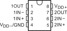
TLC2272
FK Package
FK Package
20-Pin LCCC
Top View
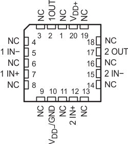
TLC2272
U Package
U Package
10-Pin CFP
Top View
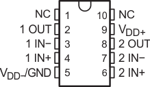
TLC2274
D, J, N, PW, or W Package
D, J, N, PW, or W Package
14-Pin SOIC, CDIP, PDIP, TSSOP, or CFP
Top View
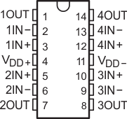
TLC2274
FK Package
FK Package
20-Pin LCCC
Top View
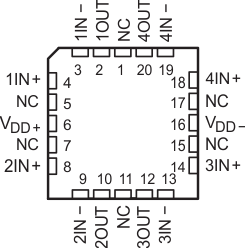
Pin Functions
| PIN | I/O | DESCRIPTION | |||||
|---|---|---|---|---|---|---|---|
| NAME | NO. | ||||||
| TLC2272 | TLC2274 | ||||||
| D, JG, P, or PW | FK | U | D, J, N, PW, or W | FK | |||
| 1IN+ | 3 | 7 | 4 | 3 | 4 | I | Non-inverting input, Channel 1 |
| 1IN- | 2 | 5 | 3 | 2 | 3 | I | Inverting input, Channel 1 |
| 1OUT | 1 | 2 | 2 | 1 | 2 | O | Output, Channel 1 |
| 2IN+ | 5 | 12 | 6 | 5 | 8 | I | Non-inverting input, Channel 2 |
| 2IN- | 6 | 15 | 7 | 6 | 9 | I | Inverting input, Channel 2 |
| 2OUT | 7 | 17 | 8 | 7 | 10 | O | Output, Channel 2 |
| 3IN+ | — | — | — | 10 | 14 | I | Non-inverting input, Channel 3 |
| 3IN- | — | — | — | 9 | 13 | I | Inverting input, Channel 3 |
| 3OUT | — | — | — | 8 | 12 | O | Output, Channel 3 |
| 4IN+ | — | — | — | 12 | 18 | I | Non-inverting input, Channel 4 |
| 4IN- | — | — | — | 13 | 19 | I | Inverting input, Channel 4 |
| 4OUT | — | — | — | 14 | 20 | O | Output, Channel 4 |
| VDD+ | 8 | 20 | 9 | 4 | 6 | — | Positive (highest) supply |
| VDD– | — | — | — | 11 | 16 | — | Negative (lowest) supply |
| VDD–/GND | 4 | 10 | 5 | — | — | — | Negative (lowest) supply |
| NC | — | 1, 3, 4, 6, 8, 9, 11, 13, 14, 16, 18, 19 | 1, 10 | — | 1, 5, 7, 11, 15, 17 | — | No Connection |