ZHCSK03J August   1983  – November 2023 TLC555

PRODUCTION DATA  

  1.   1
  2. 特性
  3. 应用
  4. 说明
  5. Pin Configuration and Functions
  6. Specifications
    1. 5.1 Absolute Maximum Ratings
    2. 5.2 ESD Ratings
    3. 5.3 Recommended Operating Conditions
    4. 5.4 Thermal Information
    5. 5.5 Electrical Characteristics: VDD = 2 V for TLC555C, VDD = 3 V for TLC555I
    6. 5.6 Electrical Characteristics: VDD = 5 V
    7. 5.7 Electrical Characteristics: VDD = 15 V
    8. 5.8 Timing Characteristics
    9. 5.9 Typical Characteristics
  7. Detailed Description
    1. 6.1 Overview
    2. 6.2 Functional Block Diagram
    3. 6.3 Feature Description
      1. 6.3.1 Monostable Operation
      2. 6.3.2 Astable Operation
      3. 6.3.3 Frequency Divider
    4. 6.4 Device Functional Modes
  8. Application and Implementation
    1. 7.1 Application Information
    2. 7.2 Typical Applications
      1. 7.2.1 Missing-Pulse Detector
        1. 7.2.1.1 Design Requirements
        2. 7.2.1.2 Detailed Design Procedure
        3. 7.2.1.3 Application Curve
      2. 7.2.2 Pulse-Width Modulation
        1. 7.2.2.1 Design Requirements
        2. 7.2.2.2 Detailed Design Procedure
        3. 7.2.2.3 Application Curve
      3. 7.2.3 Pulse-Position Modulation
        1. 7.2.3.1 Design Requirements
        2. 7.2.3.2 Detailed Design Procedure
        3. 7.2.3.3 Application Curves
      4. 7.2.4 Sequential Timer
        1. 7.2.4.1 Design Requirements
        2. 7.2.4.2 Detailed Design Procedure
        3. 7.2.4.3 Application Curve
      5. 7.2.5 Designing for Improved ESD Performance
    3. 7.3 Power Supply Recommendations
    4. 7.4 Layout
      1. 7.4.1 Layout Guidelines
      2. 7.4.2 Layout Example
  9. Device and Documentation Support
    1. 8.1 接收文档更新通知
    2. 8.2 支持资源
    3. 8.3 Trademarks
    4. 8.4 静电放电警告
    5. 8.5 术语表
  10. Revision History
  11. 10Mechanical, Packaging, and Orderable Information

封装选项

机械数据 (封装 | 引脚)
散热焊盘机械数据 (封装 | 引脚)
订购信息

Pulse-Width Modulation

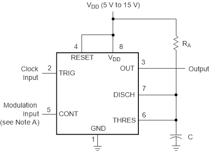
To modify timer operation, apply an external voltage (or current) to CONT to modulate the internal threshold and trigger voltages. Figure 7-3 shows a circuit for pulse-width modulation. A continuous input pulse train triggers the monostable circuit, and a control signal modulates the threshold voltage. Figure 7-4 shows the resulting duty cycle versus control voltage transfer function. Attempting to run under 10% duty cycle can result in inconsistent output pulses. Attempting to run close to 100% duty cycle results in frequency division by 2, then 3, then 4.
GUID-F30C0E2A-4634-41C2-8626-DC3B045AF288-low.gif
The modulating signal can be direct or capacitively coupled to CONT. For direct coupling, consider the effects of modulation source voltage and impedance on the bias of the timer.
Figure 7-3 Circuit for Pulse-Width Modulation