ZHCSK03J August 1983 – November 2023 TLC555
PRODUCTION DATA
- 1
- 1 特性
- 2 应用
- 3 说明
- 4 Pin Configuration and Functions
-
5 Specifications
- 5.1 Absolute Maximum Ratings
- 5.2 ESD Ratings
- 5.3 Recommended Operating Conditions
- 5.4 Thermal Information
- 5.5 Electrical Characteristics: VDD = 2 V for TLC555C, VDD = 3 V for TLC555I
- 5.6 Electrical Characteristics: VDD = 5 V
- 5.7 Electrical Characteristics: VDD = 15 V
- 5.8 Timing Characteristics
- 5.9 Typical Characteristics
- 6 Detailed Description
- 7 Application and Implementation
- 8 Device and Documentation Support
- 9 Revision History
- 10Mechanical, Packaging, and Orderable Information
封装选项
机械数据 (封装 | 引脚)
散热焊盘机械数据 (封装 | 引脚)
- PS|8
订购信息
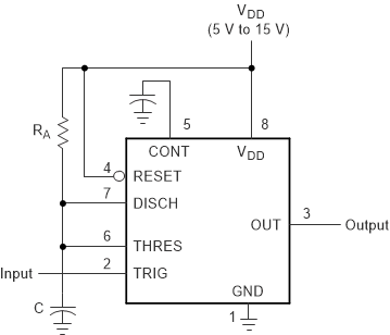
6.3.1 Monostable Operation
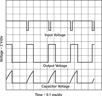
For monostable operation, Figure 6-2 shows how any of these timers can be connected. If the output is low, application of a negative-going pulse to the trigger (TRIG) sets the internal latch; the output goes high, and discharge pin (DISCH) becomes open drain. Capacitor C then is charged through RA until the voltage across the capacitor reaches the threshold voltage of the threshold (THRES) input. If TRIG has returned to a high level, the output of the threshold comparator resets the internal latch, the output goes low, the discharge pin goes low, which quickly discharges capacitor C.
 Figure 6-2 Circuit for Monostable Operation
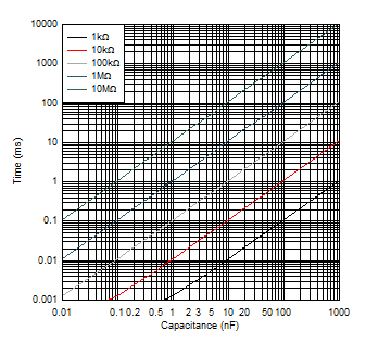
Monostable operation is initiated when TRIG voltage is less than the trigger threshold. If initiated, the sequence ends only if TRIG is high for at least 1 µs before the end of the timing interval. When the trigger is grounded, the comparator storage time can be as long as 1 µs, which limits the minimum monostable pulse duration to 1 µs. The output pulse duration is approximately tw = 1.1 × RAC. Figure 6-4 is a plot of the time constant for various values of RA and C. The threshold levels and charge rates both are directly proportional to the supply voltage, VDD. The timing interval is, therefore, independent of the supply voltage, so long as the supply voltage is constant during the time interval.
Applying a negative-going trigger pulse simultaneously to RESET and TRIG during the timing interval discharges capacitor C and reinitiates the cycle, commencing on the positive edge of the reset pulse. The output is held low as long as the reset pulse is low. To prevent false triggering, when RESET is not asserted low, RESET must be connected to VDD. If the RESET function is required and the pin is driven by external logic or a microcontroller, use a pullup resistor to VDD (such as 10 kΩ) to prevent the RESET pin from floating. If the RESET function is not required, short the RESET pin directly to the VDD pin.
In monostable applications, set the trip point of the trigger input by a voltage applied to CONT. An input voltage between 10% and 80% of the supply voltage, from a resistor divider with at least 500-µA bias, provides good results.

