SBVS146D August 2010 – December 2015 TLC5971
PRODUCTION DATA.
- 1 Features
- 2 Applications
- 3 Description
- 4 Revision History
- 5 Pin Configuration and Functions
- 6 Specifications
- 7 Parametric Measurement Information
-
8 Detailed Description
- 8.1 Overview
- 8.2 Functional Block Diagram
- 8.3 Feature Description
- 8.4 Device Functional Modes
- 8.5 Programming
- 9 Application and Implementation
- 10Power Supply Recommendations
- 11Layout
- 12Device and Documentation Support
- 13Mechanical, Packaging, and Orderable Information
封装选项
机械数据 (封装 | 引脚)
散热焊盘机械数据 (封装 | 引脚)
订购信息
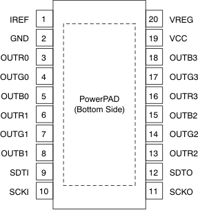
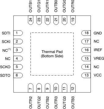
5 Pin Configuration and Functions
PWP Package
20-Pin HTSSOP
Bottom View

RGE Package
24-Pin VQFN
Bottom View

NC = not connected
Pin Functions
| PIN | I/O | DESCRIPTION | ||
|---|---|---|---|---|
| NAME | PWP | RGE | ||
| SDTI | 9 | 1 | I | Serial data input for the 224-bit shift register |
| SCKI | 10 | 2 | I | Serial data shift clock input. Data present on SDTI are shifted to the LSB of the 224-bit shift register with the SCKI rising edge Data in the shift register are shifted toward the MSB at each SCKI rising edge. The MSB data of the shift register appear on SDTO. |
| SDTO | 12 | 6 | O | Serial data output of the 224-bit shift register. SDTO is connected to the MSB of the 224-bit shift register. Data are clocked out at the SCKI rising edge. |
| SCKO | 11 | 5 | O | Serial data shift clock output. The input shift clock signal from SCKI is adjusted to the timing of the serial data output for SDTO and the signal is then output at SCKO. |
| VREG | 20 | 15 | I/O | Internal linear voltage regulator output. A decoupling capacitor of 1 µF must be connected. This output can be used for external devices as a 3.3-V power supply. This terminal can be connected with the VREG terminal of other devices to increase the supply current. Also, this pin can be supplied with 3 V to 5.5 V from an external power supply by connecting it to VCC. |
| IREF | 1 | 16 | I/O | Maximum current programming terminal. A resistor connected between IREF and GND sets the maximum current for every constant-current output. When this terminal is directly connected to GND, all outputs are forced off. The external resistor should be placed close to the device. |
| OUTR0 | 3 | 19 | O | RED constant-current outputs. Multiple outputs can be configured in parallel to increase the constant-current capability. Different voltages can be applied to each output. |
| OUTR1 | 6 | 22 | O | |
| OUTR2 | 13 | 7 | O | |
| OUTR3 | 16 | 10 | O | |
| OUTG0 | 4 | 20 | O | GREEN constant-current outputs. Multiple outputs can be configured in parallel to increase the constant-current capability. Different voltages can be applied to each output. |
| OUTG1 | 7 | 23 | O | |
| OUTG2 | 14 | 8 | O | |
| OUTG3 | 17 | 11 | O | |
| OUTB0 | 5 | 21 | O | BLUE constant-current outputs. Multiple outputs can be configured in parallel to increase the constant-current capability. Different voltages can be applied to each output. |
| OUTB1 | 8 | 24 | O | |
| OUTB2 | 15 | 9 | O | |
| OUTB3 | 18 | 12 | O | |
| VCC | 19 | 13 | — | Power-supply terminal |
| GND, PowerPAD (PWP) | 2 | — | — | Power ground terminal |
| GND, exposed thermal pad (RGE) | — | 18 | — | |
| NC | — | 3, 4, 14, 17 | — | No internal connection |