SBVS146D August 2010 – December 2015 TLC5971
PRODUCTION DATA.
- 1 Features
- 2 Applications
- 3 Description
- 4 Revision History
- 5 Pin Configuration and Functions
- 6 Specifications
- 7 Parametric Measurement Information
-
8 Detailed Description
- 8.1 Overview
- 8.2 Functional Block Diagram
- 8.3 Feature Description
- 8.4 Device Functional Modes
- 8.5 Programming
- 9 Application and Implementation
- 10Power Supply Recommendations
- 11Layout
- 12Device and Documentation Support
- 13Mechanical, Packaging, and Orderable Information
封装选项
机械数据 (封装 | 引脚)
散热焊盘机械数据 (封装 | 引脚)
订购信息
6 Specifications
6.1 Absolute Maximum Ratings
over operating free-air temperature range, unless otherwise noted.(1)(2)| MIN | MAX | UNIT | ||
|---|---|---|---|---|
| Supply voltage, VCC | –0.3 | 18 | V | |
| Input voltage | IREF | –0.3 | VREG + 0.3 | V |
| SDTI, SCKI | –0.3 | VREG + 0.6 | V | |
| Output voltage | OUTR0 to OUTR3, OUTG0 to OUTG3, OUTB0 to OUTB3 | –0.3 | 18 | V |
| SDTO, SCKO | –0.3 | VREG + 0.3 | V | |
| VREG | –0.3 | 6 | V | |
| Output current (DC) | OUTR0 to OUTR3, OUTG0 to OUTG3, OUTB0 to OUTB3 | 75 | mA | |
| VREG | –30 | mA | ||
| Operating junction temperature, TJ (max) | 150 | °C | ||
| Storage temperature, Tstg | –55 | 150 | °C | |
(1) Stresses beyond those listed under Absolute Maximum Ratings may cause permanent damage to the device. These are stress ratings only, and functional operation of the device at these or any other conditions beyond those indicated under Recommended Operating Conditions is not implied. Exposure to absolute-maximum-rated conditions for extended periods may affect device reliability.
(2) All voltage values are with respect to network ground terminal.
6.2 ESD Ratings
| VALUE | UNIT | |||
|---|---|---|---|---|
| V(ESD) | Electrostatic discharge | Human body model (HBM), per ANSI/ESDA/JEDEC JS-001(1) | ±4000 | V |
| Charged-device model (CDM), per JEDEC specification JESD22-C101(2) | ±2000 | |||
(1) JEDEC document JEP155 states that 500-V HBM allows safe manufacturing with a standard ESD control process.
(2) JEDEC document JEP157 states that 250-V CDM allows safe manufacturing with a standard ESD control process.
6.3 Recommended Operating Conditions
at TA = –40°C to +85°C, and VCC = 6 V to 17 V or VCC = VREG = 3 V to 5.5 V, unless otherwise noted.| MIN | NOM | MAX | UNIT | ||
|---|---|---|---|---|---|
| DC CHARACTERISTICS | |||||
| VCC | Supply voltage, internal voltage regulator used | 6 | 17 | V | |
| VREG | Supply voltage, VREG connected to VCC | 3 | 3.3 | 5.5 | V |
| VO | Voltage applied to output (OUTR0 to OUTR3, OUTG0 to OUTG3, OUTB0 to OUTB3) |
17 | V | ||
| VIH | High-level input voltage (SDTI, SCKI) | 0.7 × VREG | VREG | V | |
| VIL | Low-level input voltage (SDTI, SCKI) | GND | 0.3 × VREG | V | |
| VIHYS | Input voltage hysteresis (SDTI, SCKI) | 0.2 × VREG | V | ||
| IOH | High-level output current (SDTO) | –2 | mA | ||
| IOL | Low-level output current (SDTO) | 2 | mA | ||
| IOLC | Constant output sink current (OUTR0 to OUTR3, OUTG0 to OUTG3, OUTB0 to OUTB3) |
60 | mA | ||
| IREG | Voltage regulator output current (VREG) | –25 | mA | ||
| TA | Operating free temperature range | –40 | 85 | °C | |
| TJ | Operating junction temperature | –40 | 125 | °C | |
| AC CHARACTERISTICS | |||||
| fCLK (SCKI) | Data clock frequency and GS control clock frequency, SCKI | 0.007 | 20 | MHz | |
| tWH/tWL | Pulse duration, SCKI | 10 | ns | ||
| tSU | Setup time, SDTI – SCKI↑ | 5 | ns | ||
| tH | Hold time, SDTI – SCKI↑ | 3 | ns | ||
6.4 Thermal Information
| THERMAL METRIC(1) | TLC5971 | UNIT | ||
|---|---|---|---|---|
| PWP (HTSSOP) | RGE (VQFN) | |||
| 20 PINS | 24 PINS | |||
| θJA | Junction-to-ambient thermal resistance | 68.6 | 38 | °C/W |
| θJCtop | Junction-to-case (top) thermal resistance | 44.2 | 40.5 | °C/W |
| θJB | Junction-to-board thermal resistance | 19.3 | 10.2 | °C/W |
| ψJT | Junction-to-top characterization parameter | 2.7 | 0.3 | °C/W |
| ψJB | Junction-to-board characterization parameter | 15.7 | 10 | °C/W |
| θJCbot | Junction-to-case (bottom) thermal resistance | 1.8 | 2.9 | °C/W |
(1) For more information about traditional and new thermal metrics, see the Semiconductor and IC Package Thermal Metrics application report, SPRA953.
6.5 Electrical Characteristics
At TA = –40°C to +85°C, VCC = 6 V to 17 V or VCC = VREG = 3 V to 5.5 V, VLED = 5 V, and CVREG = 1 µF, unless otherwise noted. Typical values are at TA = 25°C and VCC = 12 V.| PARAMETER | TEST CONDITIONS | MIN | TYP | MAX | UNIT | |
|---|---|---|---|---|---|---|
| VOH | High-level output voltage, SDTO/SCKO | IOH = –2 mA | VREG – 0.4 | VREG | V | |
| VOL | Low-level output voltage, SDTO/SCKO | IOL = 2 mA | 0 | 0.4 | V | |
| II | Input current, SDTI/SCKI | VI = VREG or GND | –1 | 1 | µA | |
| ICC | Supply current | SDTI/SCKI = low, BLANK = 1, GSn = FFFFh, BCX = 7Fh, VOUTXn = 1 V, RIREF = 24 kΩ (IOLCMax = 2 mA) |
2 | 4 | mA | |
| ICC1 | SDTI/SCKI = low, BLANK = 1, GSn = FFFFh, BCX = 7Fh, VOUTXn = 1 V, RIREF = 1.6 kΩ (IOLCMax = 30 mA) |
6 | 9 | mA | ||
| ICC2 | SDTI = 10 MHz, SCKI = 20 MHz, BLANK = 0, auto repeat enable, external GS clock selected, GSn = FFFFh, BCX = 7Fh, VOUTXn = 1 V, RIREF = 1.6 kΩ (IOLCMax = 30 mA) |
14 | 22 | mA | ||
| ICC3 | SDTI = 10 MHz, SCKI = 20 MHz, BLANK = 0, auto repeat enable, external GS clock selected, GSn = FFFFh, BCX = 7Fh, VOUTXn = 1 V, RIREF = 0.82 kΩ (IOLCMax = 60 mA) |
21 | 36 | mA | ||
| IOLC | Constant output current, OUTXn | All OUTXn on, BCX = 7Fh, VOUTXn = 1 V, VOUTfix = 1 V, RIREF = 0.82 kΩ (IOLCMax = 60 mA) |
56.3 | 60.5 | 64.7 | mA |
| IOLKG | Leakage output current, OUTXn | All OUTXn off, BCX = 7Fh, VOUTXn = 17 V, VOUTfix = 17 V, RIREF = 0.82 kΩ (IOLCMax = 60 mA) |
0.1 | µA | ||
| ΔIOLC | Constant-current error(1)
(channel-to-channel in same color group), OUTXn |
All OUTXn on, BCX = 7Fh, VOUTXn = VOUTfix = 1 V, RIREF = 0.82 kΩ (IOLCMax = 60 mA) |
–3% | ±1% | 3% | |
| ΔIOLC1 | Constant current error(2)
(device-to-device in same color group), OUTXn |
All OUTXn on, BCX = 7Fh, VOUTXn = VOUTfix = 1V, RIREF = 0.82 kΩ (IOLCMax = 60 mA), at same grouped color output of OUTR0-3, OUTG0-3, and OUTB0-3 |
–4% | ±1 | 4% | |
| ΔIOLC2 | Line regulation of constant-current output, OUTXn(3) | All OUTn on, BCX = 7Fh, VOUTXn = VOUTfix = 1 V, RIREF = 0.82 kΩ (IOLCMax = 60 mA) |
–1 | ±0.5 | 1 | %/V |
| ΔIOLC3 | Load regulation of constant-current output, OUTXn(4) | All OUTn on, BCX = 7Fh, VOUTXn = VOUTfix = 1 V, RIREF = 0.82 kΩ (IOLCMax = 60 mA) |
–3 | ±1 | 3 | %/V |
| TTSD | Thermal shutdown temperature | Junction temperature(5) | 150 | 165 | 180 | °C |
| THYS | Thermal shutdown hysteresis | Junction temperature(5) | 5 | 10 | 20 | °C |
| VIREF | Reference voltage output, IREF | RIREF = 0.82 kΩ | 1.18 | 1.21 | 1.24 | V |
| VREG | Linear regulator output voltage, VREG | VCC = 6 V to 17 V, IREG = 0 mA to –25 mA | 3.1 | 3.3 | 3.5 | V |
| ΔVREG | Line regulation of linear regulator, VREG | VCC = 6 V to 17 V, IREG = 0 mA | 90 | mV | ||
| ΔVREG1 | Load regulation of linear regulator, VREG | VCC = 12 V, IREG = 0 mA to –25 mA | 120 | mV | ||
| VSTR | Undervoltage lockout release, VREG | 2.5 | 2.7 | 2.9 | V | |
| VHYS | Undervoltage lockout hysteresis, VREG | 300 | 400 | 500 | mV | |
(1)
| The deviation of each output in the same color group (OUTR0-OUTR3 or OUTG0-OUTG3 or OUTB0-OUTB3) from the average current from the same color group. Deviation is calculated by Equation 1: | ||
|
Equation 1.
 where
|
(2)
| The deviation of each color group constant-current average from the ideal constant-current value. Deviation is calculated by Equation 2: | ||
|
Equation 2.
 where
|
||
| Ideal current is calculated by Equation 3 for the OUTRn and OUTGn groups: | ||
|
Equation 3.
 where
|
(3)
| Line regulation is calculated by Equation 4: | ||
|
Equation 4.
 where
|
(4)
| Load regulation is calculated by Equation 5: | ||
|
Equation 5.
 where
|
(5) Not tested, specified by design.
(6) The propagation delays are calculated by tD2 = tD0 – tD1.
(7) The generation timing of the internal latch pulse changes depending on the SCKI clock frequency; see the Internal Latch Pulse Generation Timing section.
6.6 Switching Characteristics
At TA = –40°C to +85°C, VCC = 6 V to 17 V or VCC = VREG = 3 V to 5.5 V, CVREG = 1 µF, CL = 15 pF, RL = 68 Ω, and VLED = 5 V, unless otherwise noted. Typical values are at TA = 25°C and VCC = 12 V.| PARAMETER | TEST CONDITIONS | MIN | TYP | MAX | UNIT | |
|---|---|---|---|---|---|---|
| tR0 | Rise time, SDTO/SCKO | 3 | 10 | ns | ||
| tR1 | Rise time, OUTXn | BCX = 7Fh | 5 | 15 | ns | |
| tF0 | Fall time, SDTO/SCKO | 3 | 10 | ns | ||
| tF1 | Fall time, OUTXn | BCX = 7Fh | 15 | 25 | ns | |
| tD0 | Propagation delay | SCKI↑ to SDTO↑↓ | 10 | 25 | 60 | ns |
| tD1 | SCKI↑ to SCKO↑ | 5 | 15 | 40 | ns | |
| tD2(6) | SCKO↑ to SDTO↑↓ | 5 | 10 | 20 | ns | |
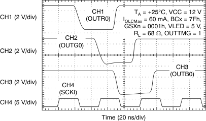
| tD3 | SCKI↑ to OUTRn↑↓, BLANK = 0, BCXn = 7Fh, OUTTMG = 1 Or SCKI↓ to OUTRn↑↓, BLANK = 0, BCXn = 7Fh, OUTTMG = 0 |
10 | 25 | 60 | ns | |
| tD4 | SCKI↑ to OUTGn↑↓, BLANK = 0, BCXn = 7Fh, OUTTMG = 1 Or SCKI↓ to OUTGn↑↓, BLANK = 0, BCXn = 7Fh, OUTTMG = 0 |
25 | 50 | 90 | ns | |
| tD5 | SCKI↑ to OUTBn↑↓, BLANK = 0, BCXn = 7Fh, OUTTMG = 1 Or SCKI↓ to OUTBn↑↓, BLANK = 0, BCXn = 7Fh, OUTTMG = 0 |
40 | 75 | 120 | ns | |
| tD6(7) | Last SCKI↑ to internal latch pulse genaration | 8/fOSC | 16384/fOSC | s | ||
| tW(SCKO) | Shift clock output one pulse width | SCKO↑ to SCKO↓ | 12 | 25 | 35 | ns |
| fOSC | Internal oscillator frequency | 6 | 10 | 12 | MHz | |
6.7 Dissipation Ratings
| PACKAGE | DERATING FACTOR ABOVE TA = 25°C |
POWER RATING TA < 25°C |
POWER RATING TA = 70°C |
POWER RATING TA = 85°C |
|---|---|---|---|---|
| HTSSOP 20-pin with PowerPAD soldered(1) | 25.7 mW/°C | 3121 mW | 1998 mW | 1623 mW |
| QFN 24-pin exposed thermal pad soldered(2) | 24.8 mW/°C | 3106 mW | 1988 mW | 1615 mW |
(1) With PowerPAD soldered onto copper area on TI recommended printed circuit board (PCB); 2-oz. copper. For more information, see application report PowerPAD Thermally-Enhanced Package (SLMA002) available for download at www.ti.com.
(2) The package thermal impedance is calculated in accordance with JESD51-5.
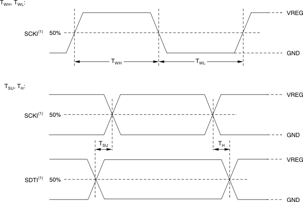
1. Input pulse rise and fall time is 1 ns to 3 ns.
Figure 1. Input Timing
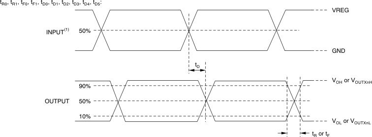
1. Input pulse rise and fall time is 1 ns to 3 ns.
Figure 2. Output Timing
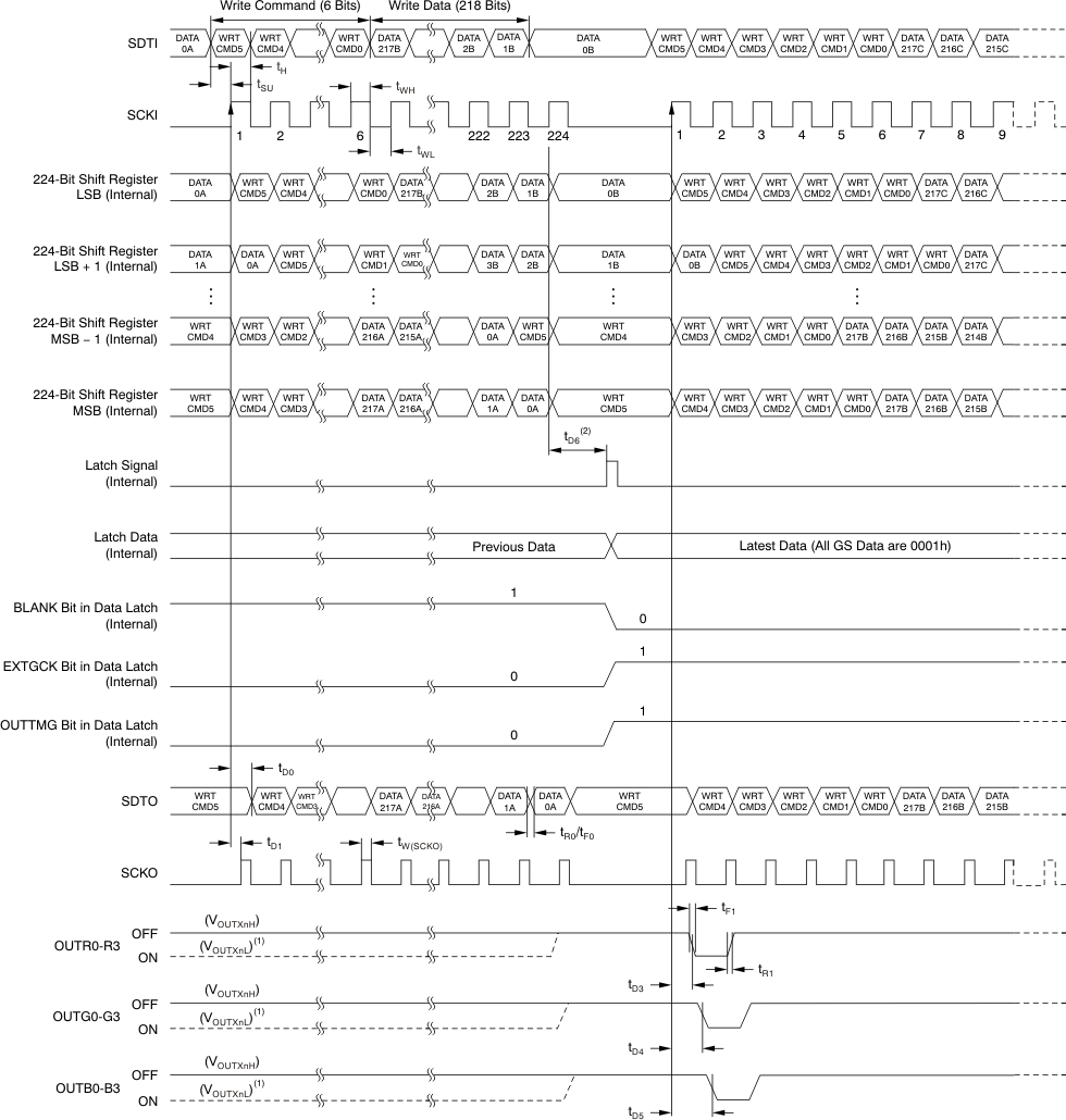
1. OUTXn ON-OFF timing depends on previous GS data in the 218-bit data latch.
2. The propagation delay time shows the period from the rising edge of the last SCKI, not the 224th SCKI to the internal latch signal generation.
Figure 3. Data Write and OUTXn Switching Timing (OUTTMG = 1)
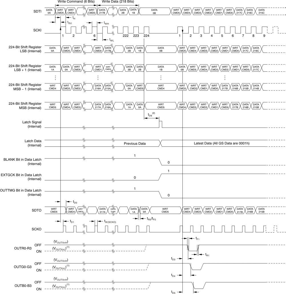
1. OUTXn ON-OFF timing depends on previous GS data in the 218-bit data latch.
2. The propagation delay time shows the period from the rising edge of the last SCKI, not the 224th SCKI to the internal latch signal generation.
Figure 4. Data Write and OUTXn Switching Timing (OUTTMG = 0)
6.8 Typical Characteristics
At TA = 25°C and VCC = 24 V, unless otherwise noted.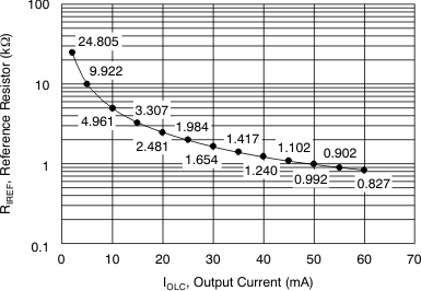 Figure 5. Reference Resistor vs Output Current
 Figure 7. Output Current vs Output Voltage
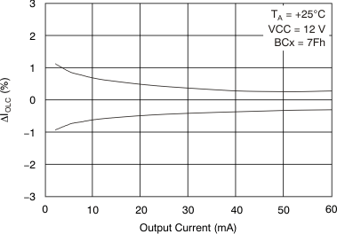 Figure 9. Constant-Current Error vs Output Current
(Channel-to-Channel in Color Group)
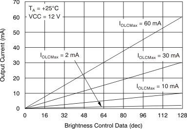 Figure 11. Global Brightness Control Linearity
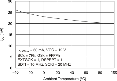 Figure 13. Supply Current vs Ambient Temperature
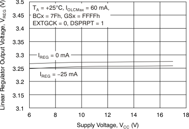 Figure 15. Linear Regulator Output Voltage vs Supply Voltage
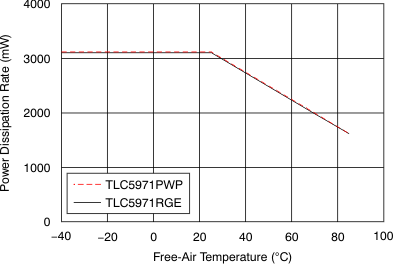 Figure 6. Power Dissipation vs Temperature
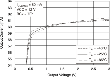 Figure 8. Output Current vs Output Voltage
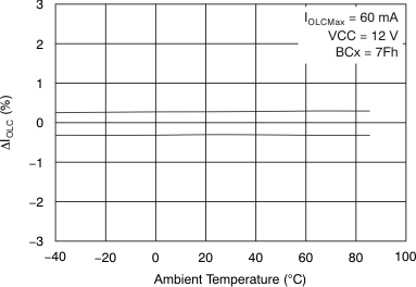 Figure 10. Constant-Current Error vs Ambient Temperature
(Channel-to-Channel in Color Group)
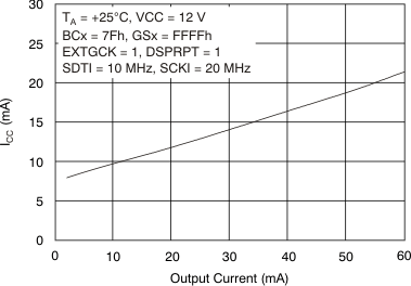 Figure 12. Supply Current vs Output Current
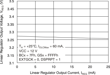 Figure 14. Linear Regulator Output Voltage vs Linear Regulator Output Current
