ZHCSPI8D November   2021  – July 2022 TLC6984

PRODUCTION DATA  

  1. 特性
  2. 应用
  3. 说明
  4. Revision History
  5. 说明(续)
  6. Pin Configuration and Functions
  7. Specifications
    1. 7.1 Absolute Maximum Ratings
    2. 7.2 ESD Ratings
    3. 7.3 Recommended Operating Conditions
    4. 7.4 Thermal Information
    5. 7.5 Electrical Characteristics
    6. 7.6 Timing Requirements
    7. 7.7 Switching Characteristics
    8. 7.8 Typical Characteristics
  8. Detailed Description
    1. 8.1 Overview
    2. 8.2 Functional Block Diagram
    3. 8.3 Feature Description
      1. 8.3.1 Independent and Stackable Mode
        1. 8.3.1.1 Independent Mode
        2. 8.3.1.2 Stackable Mode
      2. 8.3.2 Current Setting
        1. 8.3.2.1 Brightness Control (BC) Function
        2. 8.3.2.2 Color Brightness Control (CC) Function
        3. 8.3.2.3 Choosing BC/CC for a Different Application
      3. 8.3.3 Frequency Multiplier
      4. 8.3.4 Line Transitioning Sequence
      5. 8.3.5 Protections and Diagnostics
        1. 8.3.5.1 Thermal Shutdown Protection
        2. 8.3.5.2 IREF Resistor Short Protection
        3. 8.3.5.3 LED Open Load Detection and Removal
          1. 8.3.5.3.1 LED Open Detection
          2. 8.3.5.3.2 Read LED Open Information
          3. 8.3.5.3.3 LED Open Caterpillar Removal
        4. 8.3.5.4 LED Short and Weak Short Circuitry Detection and Removal
          1. 8.3.5.4.1 LED Short and Weak Short Detection
          2. 8.3.5.4.2 Read LED Short Information
          3. 8.3.5.4.3 LSD Caterpillar Removal
    4. 8.4 Device Functional Modes
    5. 8.5 Continuous Clock Series Interface
      1. 8.5.1 Data Validity
      2. 8.5.2 CCSI Frame Format
      3. 8.5.3 Write Command
        1. 8.5.3.1 Chip Index Write Command
        2. 8.5.3.2 VSYNC Write Command
        3. 8.5.3.3 MPSM Write Command
        4. 8.5.3.4 Standby Clear and Enable Command
        5. 8.5.3.5 Soft_Reset Command
        6. 8.5.3.6 Data Write Command
      4. 8.5.4 Read Command
    6. 8.6 PWM Grayscale Control
      1. 8.6.1 Grayscale Data Storage and Display
        1. 8.6.1.1 Memory Structure Overview
        2. 8.6.1.2 Details of Memory Bank
        3. 8.6.1.3 Write a Frame Data into Memory Bank
      2. 8.6.2 PWM Control for Display
    7. 8.7 Register Maps
      1. 8.7.1  FC0
      2. 8.7.2  FC1
      3. 8.7.3  FC2
      4. 8.7.4  FC3
      5. 8.7.5  FC4
      6. 8.7.6  FC14
      7. 8.7.7  FC15
      8. 8.7.8  FC16
      9. 8.7.9  FC17
      10. 8.7.10 FC18
      11. 8.7.11 FC19
      12. 8.7.12 FC20
      13. 8.7.13 FC21
  9. Application and Implementation
    1. 9.1 Application Information
    2. 9.2 Typical Application
      1. 9.2.1 Design Requirements
        1. 9.2.1.1 System Structure
        2. 9.2.1.2 SCLK Frequency
        3. 9.2.1.3 Internal GCLK Frequency
        4. 9.2.1.4 Line Switch Time
        5. 9.2.1.5 Blank Time Removal
        6. 9.2.1.6 BC and CC
      2. 9.2.2 Detailed Design Procedure
        1. 9.2.2.1 Chip Index Command
        2. 9.2.2.2 FC Registers Settings
        3. 9.2.2.3 Grayscale Data Write
        4. 9.2.2.4 VSYNC Command
        5. 9.2.2.5 LED Open and Short Read
      3. 9.2.3 Application Curves
  10. 10Power Supply Recommendations
  11. 11Layout
    1. 11.1 Layout Guidelines
    2. 11.2 Layout Example
  12. 12Device and Documentation Support
    1. 12.1 Documentation Support
      1. 12.1.1 Related Documentation
    2. 12.2 接收文档更新通知
    3. 12.3 支持资源
    4. 12.4 Trademarks
    5. 12.5 Electrostatic Discharge Caution
    6. 12.6 术语表
  13. 13Mechanical, Packaging, and Orderable Information

封装选项

机械数据 (封装 | 引脚)
散热焊盘机械数据 (封装 | 引脚)
订购信息

Independent Mode

Figure 8-1 shows an implementation of a 16 × 32 RGB LED matrix using two TLC6984s in independent mode. Each device is responsible for its own 16 ×16 RGB LED matrix which means that all the data for section A is stored in device 1 and the data for section B is stored in device 2.
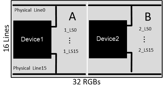
GUID-163E22C4-E9DA-483C-8EAE-D77A33388E08-low.gifFigure 8-1 Two Devices in Independent Mode

The unused line must be assigned to the last several lines of the device. For example, if there are only 14 scanning lines, then the two unused lines must be assigned to 1_LS14 and 1_LS15.