ZHCSPI8D November   2021  – July 2022 TLC6984

PRODUCTION DATA  

  1. 特性
  2. 应用
  3. 说明
  4. Revision History
  5. 说明(续)
  6. Pin Configuration and Functions
  7. Specifications
    1. 7.1 Absolute Maximum Ratings
    2. 7.2 ESD Ratings
    3. 7.3 Recommended Operating Conditions
    4. 7.4 Thermal Information
    5. 7.5 Electrical Characteristics
    6. 7.6 Timing Requirements
    7. 7.7 Switching Characteristics
    8. 7.8 Typical Characteristics
  8. Detailed Description
    1. 8.1 Overview
    2. 8.2 Functional Block Diagram
    3. 8.3 Feature Description
      1. 8.3.1 Independent and Stackable Mode
        1. 8.3.1.1 Independent Mode
        2. 8.3.1.2 Stackable Mode
      2. 8.3.2 Current Setting
        1. 8.3.2.1 Brightness Control (BC) Function
        2. 8.3.2.2 Color Brightness Control (CC) Function
        3. 8.3.2.3 Choosing BC/CC for a Different Application
      3. 8.3.3 Frequency Multiplier
      4. 8.3.4 Line Transitioning Sequence
      5. 8.3.5 Protections and Diagnostics
        1. 8.3.5.1 Thermal Shutdown Protection
        2. 8.3.5.2 IREF Resistor Short Protection
        3. 8.3.5.3 LED Open Load Detection and Removal
          1. 8.3.5.3.1 LED Open Detection
          2. 8.3.5.3.2 Read LED Open Information
          3. 8.3.5.3.3 LED Open Caterpillar Removal
        4. 8.3.5.4 LED Short and Weak Short Circuitry Detection and Removal
          1. 8.3.5.4.1 LED Short and Weak Short Detection
          2. 8.3.5.4.2 Read LED Short Information
          3. 8.3.5.4.3 LSD Caterpillar Removal
    4. 8.4 Device Functional Modes
    5. 8.5 Continuous Clock Series Interface
      1. 8.5.1 Data Validity
      2. 8.5.2 CCSI Frame Format
      3. 8.5.3 Write Command
        1. 8.5.3.1 Chip Index Write Command
        2. 8.5.3.2 VSYNC Write Command
        3. 8.5.3.3 MPSM Write Command
        4. 8.5.3.4 Standby Clear and Enable Command
        5. 8.5.3.5 Soft_Reset Command
        6. 8.5.3.6 Data Write Command
      4. 8.5.4 Read Command
    6. 8.6 PWM Grayscale Control
      1. 8.6.1 Grayscale Data Storage and Display
        1. 8.6.1.1 Memory Structure Overview
        2. 8.6.1.2 Details of Memory Bank
        3. 8.6.1.3 Write a Frame Data into Memory Bank
      2. 8.6.2 PWM Control for Display
    7. 8.7 Register Maps
      1. 8.7.1  FC0
      2. 8.7.2  FC1
      3. 8.7.3  FC2
      4. 8.7.4  FC3
      5. 8.7.5  FC4
      6. 8.7.6  FC14
      7. 8.7.7  FC15
      8. 8.7.8  FC16
      9. 8.7.9  FC17
      10. 8.7.10 FC18
      11. 8.7.11 FC19
      12. 8.7.12 FC20
      13. 8.7.13 FC21
  9. Application and Implementation
    1. 9.1 Application Information
    2. 9.2 Typical Application
      1. 9.2.1 Design Requirements
        1. 9.2.1.1 System Structure
        2. 9.2.1.2 SCLK Frequency
        3. 9.2.1.3 Internal GCLK Frequency
        4. 9.2.1.4 Line Switch Time
        5. 9.2.1.5 Blank Time Removal
        6. 9.2.1.6 BC and CC
      2. 9.2.2 Detailed Design Procedure
        1. 9.2.2.1 Chip Index Command
        2. 9.2.2.2 FC Registers Settings
        3. 9.2.2.3 Grayscale Data Write
        4. 9.2.2.4 VSYNC Command
        5. 9.2.2.5 LED Open and Short Read
      3. 9.2.3 Application Curves
  10. 10Power Supply Recommendations
  11. 11Layout
    1. 11.1 Layout Guidelines
    2. 11.2 Layout Example
  12. 12Device and Documentation Support
    1. 12.1 Documentation Support
      1. 12.1.1 Related Documentation
    2. 12.2 接收文档更新通知
    3. 12.3 支持资源
    4. 12.4 Trademarks
    5. 12.5 Electrostatic Discharge Caution
    6. 12.6 术语表
  13. 13Mechanical, Packaging, and Orderable Information

封装选项

机械数据 (封装 | 引脚)
散热焊盘机械数据 (封装 | 引脚)
订购信息

PWM Control for Display

To increase the refresh rate in time-multiplexing display system, an DS-PWM (Dynamic Spectrum- Pulse Width Modulation) algorithm is proposed in this device. One frame is divided into many segments shown as below. Note that one frame is divided into n sub-periods, n is set by SUBP_NUM (FC0 register bit24-22), and each sub-period is divided into 32 segments for 32 scan lines. Each segment contains GS GCLKs time for grayscale data display and T_SW GCLKs time for switching lines. GS is configured by the SEG_LENGTH (FC1 register bit9-0 in Table 8-8) , and T_SW is the line switch time, which is configured by the LINE_SWT (see FC1 register bit 40-37 in Table 8-8).
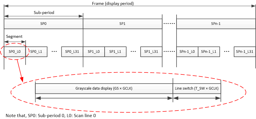
GUID-F86162AD-374D-4565-AA0D-8826A7365C55-low.gifFigure 8-28 DS-PWM Algorithm with 32 Scan Lines

The DS-PWM can not only increase the refresh rate meanwhile keep the same frame rate, but also decrease the brightness loss in low grayscale, which can smoothly increase the sub-period number when the grayscale data increases.

To achieve ultra-low luminance, the LED driver must have the ability to output a very short current pulse (1 GCLK time). However, because of the parasitic capacitor of the LEDs, such pulse can not turn on the LEDs. And the larger GCLK frequency is, the harder to turn on LEDs.

The DS-PWM algorithm has a parameter called sub-period threshold, which is used to calculate when to change sub-period number according to the giving grayscale data. Sub-period threshold defines the LED minimum turn-on time, so as to conquer the current loss caused by LED parasitic capacitor. Sub-period threshold is configured by the SUBP_TH_R/G/B (FC1 register bit24-10 in Table 8-8).

With DS-PWM algorithm, the brightness has smoothly increased with the gradient grayscale data.