ZHCSIG2A July 2018 – August 2018 TLC6C5716-Q1
PRODUCTION DATA.
- 1 特性
- 2 应用
- 3 说明
- 4 修订历史记录
- 5 Pin Configuration and Functions
- 6 Specifications
-
7 Detailed Description
- 7.1 Overview
- 7.2 Functional Block Diagram
- 7.3
Feature Description
- 7.3.1 Maximum Constant-Sink-Current Setting
- 7.3.2 Brightness Control and Dot Correction
- 7.3.3 Grayscale Configuration
- 7.3.4
Diagnostics
- 7.3.4.1 LED Diagnostics
- 7.3.4.2 Adjacent-Pin-Short Check
- 7.3.4.3 IREF-Short and IREF-Open Detection
- 7.3.4.4 Pre-Thermal Warning Flag
- 7.3.4.5 Thermal Error Flag
- 7.3.4.6 Negate-Bit Toggle
- 7.3.4.7 LOD_LSD Self-Test
- 7.3.4.8 ERR Pin
- 7.3.4.9 ERROR Clear
- 7.3.4.10 Global Reset
- 7.3.4.11 Slew Rate Control
- 7.3.4.12 Channel Group Delay
- 7.4 Device Functional Modes
- 7.5 Programming
- 7.6 Register Maps
- 8 Application and Implementation
- 9 Power Supply Recommendations
- 10Layout
- 11器件和文档支持
- 12机械、封装和可订购信息
6.5 Electrical Characteristics
VCC = 3 V to 5.5 V, TJ=–40°Cto150°C,VSENSE = 5 V, GS = FFFh, BC = FFh, DC = 7Fh with upper dotcorrection(DC)range (unless otherwise noted)| PARAMETER | TEST CONDITIONS | MIN | TYP | MAX | UNIT | |
|---|---|---|---|---|---|---|
| POWER SUPPLIES (VCC, GND) | ||||||
| ICC | Supply current | SDI, SCK, LATCH = L, BLANK = L, GCLK = L, VOUT = 1 V, IOUT = 2 mA | 4.2 | 5.5 | mA | |
| SDI, SCK, LATCH = L, BLANK = L, GCLK = L, VOUT = 1 V, IOUT = 20 mA | 7.7 | 9 | ||||
| SDI, SCK, LATCH = L, BLANK = H, GCLK = 8 MHz, VOUT = 1 V, IOUT = 20 mA , auto-repeat on | 8.3 | 10 | ||||
| SDI, SCK, LATCH = L, BLANK = H, GCLK = 8 MHz, VOUT = 1 V, IOUT = 50 mA , auto-repeat on | 13.5 | 16 | ||||
| LOGIC INPUTS (SDI, SCK, LATCH, GCLK, BLANK) | ||||||
| IIkg | Input leakage current | VI at SCK, LATCH, GCLK = VCC; VI at SDI, SCK, LATCH, BLANK, GCLK = GND | –1 | 1 | µA | |
| Rpd | Pulldown resistance at BLANK, GCLK | 250 | 500 | 750 | kΩ | |
| CONTROL OUTPUTS (IREF, ERR, SDO) | ||||||
| VIREF | IREF voltage | RIREF = 0.96 kΩ | 1.17 | 1.2 | 1.23 | V |
| VOH | High-level output voltage | At SDO, IOH = –1 mA | VCC – 0.4 | VCC | V | |
| VOL | Low-level output voltage | At SDO, IOL = 1 mA | 0.4 | V | ||
| VERR | ERR pin open-drain voltage drop | IERR = 4 mA | 0.1 VCC | V | ||
| Ilkg(ERR) | ERR pin leakage current | VERR = 5 V | 1 | µA | ||
| OUTPUT STAGE | ||||||
| V(OUT,min) | Minimum output voltage | VCC = 3.6 V, IOUT = 50 mA | 0.67 | V | ||
| VCC = 3 V, IOUT = 50 mA | 0.7 | |||||
| K(OUT) | Ratio of output current to IREF current, K = I(OUTx) / I(IREF) | 40 | mA/mA | |||
| Ilkg(OUT) | Output leakage current | BLANK = L, VOUT = 7 V, VSENSE = 7 V, IOUT = 50 mA | 0.1 | µA | ||
| CHANNEL ACCURACY | ||||||
| I(OUT) | Constant output current | VOUT = 1 V, RIREF = 24 kΩ | 1.86 | 2 | 2.14 | mA |
| VOUT = 1 V, RIREF = 0.96 kΩ | 46.5 | 50 | 53.5 | |||
| VOUT = 1V, RIREF open or short | 7 | 10 | 13 | |||
| ΔI(Ch-Ch)(1) | Current accuracy (channel-to-channel in same color group) | VOUT = 1 V, IOUT = 50 mA | –4% | 4% | ||
| VOUT = 1 V, IOUT = 2 mA | –4% | 4% | ||||
| ΔI(Dev-Dev)(2) | Current accuracy (device-to-device) | VOUT= 1 V, IOUT = 50 mA | –4% | 4% | ||
| VOUT = 1 V, IOUT = 2 mA | –4% | 4% | ||||
| ΔI(Ch-Ideal)(3) | Current accuracy (channel-to-ideal output) | VOUT = 1 V, IOUT = 50 mA | –7% | 7% | ||
| VOUT = 1 V, IOUT = 2 mA | –7% | 7% | ||||
| ΔI(OUT-VCC)(4) | Line regulation | VOUT = 1 V, IOUT = 50 mA | –0.7 | 0.7 | %/V | |
| VOUT = 1 V, IOUT = 2 mA | –0.7 | 0.7 | ||||
| ΔI(OUT-VOUT)(5) | Load regulation | VOUT = 1 V to 3 V, IOUT = 50 mA | –0.7 | 0.7 | ||
| VOUT = 1 V to 3 V, IOUT = 2 mA | –0.7 | 0.7 | ||||
| PROTECTION CIRCUITS | ||||||
| VLOD | LED open-circuit detection threshold | LOD_VOLTAGE = 0b | 0.275 | 0.3 | 0.32 | V |
| LOD_VOLTAGE = 1b | 0.48 | 0.5 | 0.52 | |||
| VLSD | LED short-circuit detection threshold | LSD_VOLTAGE = 0b | VSENSE – 0.4 | VSENSE – 0.3 | VSENSE – 0.2 | V |
| LSD_VOLTAGE = 1b | VSENSE – 0.8 | VSENSE – 0.7 | VSENSE – 0.6 | |||
| IIREF_OC | IREF resistor open-circuit detection threshold | VCC = 5 V | 8 | 10 | 12 | µA |
| IIREF_OCHYS | IREF resistor open-circuit detection threshold hysteresis | VCC = 5 V | 5 | µA | ||
| IIREF_SC | IREF resistor short-circuit-detection threshold | VCC = 5 V | 2 | 2.7 | 3.2 | mA |
| IIREF_SCHYS | IREF resistor short-circuit-detection threshold hysteresis | VCC = 5 V | 0.3 | mA | ||
| TPTW | Pre-thermal warning flag threshold | 125 | 135 | 145 | °C | |
| THYS_PTW | Pre-thermal warning flag hysteresis | 10 | °C | |||
| TSD | Thermal error flag threshold | 150 | 160 | 170 | °C | |
| THYS_TEF | Thermal error flag hysteresis | 10 | °C | |||
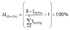
(1) Channel to channel accuracy in the same color group iscalculated by the formula below. (X = color group; i,j = 0 to 7 )


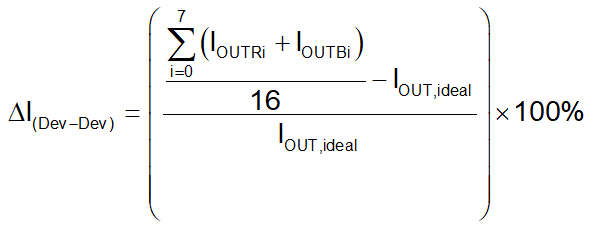
(2) Device to device accuracy is calculated by the formulabelow.


(3) Channel to ideal accuracy is calculated by the formulabelow.


(4) Line regulation accuracy is calculated by the formulabelow.


(5) Load regulation accuracy is calculated by the formulabelow.

