ZHCSIO0A December 2017 – August 2018 TLC6C5724-Q1
PRODUCTION DATA.
- 1 特性
- 2 应用
- 3 说明
- 4 修订历史记录
- 5 Pin Configuration and Functions
- 6 Specifications
-
7 Detailed Description
- 7.1 Overview
- 7.2 Functional Block Diagram
- 7.3
Feature Description
- 7.3.1 Maximum Constant-Sink-Current Setting
- 7.3.2 Brightness Control and Dot Correction
- 7.3.3 Grayscale Configuration
- 7.3.4
Diagnostics
- 7.3.4.1 LED Diagnostics
- 7.3.4.2 Adjacent-Pin-Short Check
- 7.3.4.3 IREF Short and IREF Open Detection
- 7.3.4.4 Pre-Thermal Warning Flag
- 7.3.4.5 Thermal Error Flag
- 7.3.4.6 Negate Bit Toggle
- 7.3.4.7 LOD_LSD Self-Test
- 7.3.4.8 ERR Pin
- 7.3.4.9 ERROR Clear
- 7.3.4.10 Global Reset
- 7.3.4.11 Slew Rate Control
- 7.3.4.12 Channel Group Delay
- 7.4 Device Functional Modes
- 7.5 Programming
- 7.6 Register Maps
- 8 Application and Implementation
- 9 Power Supply Recommendations
- 10Layout
- 11器件和文档支持
- 12机械、封装和可订购信息
7.3.4.1 LED Diagnostics
An LOD-LSD detection circuit compares the output voltage with the LOD threshold and LSD threshold, and the output results show in Table 1.
Table 1. LOD-LSD Detection
| OUTPUT VOLTAGE CONDITION | DETECTOR OUTPUT BIT VALUE | |
|---|---|---|
| LOD | LSD | |
| VOUTn < LOD_VOLTAGE | 1 | 0 |
| LOD_VOLTAGE < VOUTn < LSD_VOLTAGE | 0 | 0 |
| VOUTn > LSD_VOLTAGE | 0 | 1 |
The LOD threshold can be configured by the LOD_VOLTAGE bit. The threshold is 0.3 V when LOD_VOLTAGE = 0, and the threshold is 0.5 V when LOD_VOLTAGE = 1.
LSD threshold is configured by the LSD_VOLTAGE bit. The threshold is VVSENSE – 0.3 V when LSD_VOLTAGE = 0, and the threshold is VSENSE – 0.7 V when LSD_VOLTAGE = 1.
There are two sets of LOD-LSD registers in the device. One is the LOD1-LSD1 registers, another is the LOD2-LSD2 registers. Each group of registers consists of 24 bits of LOD data and 24 bits of LSD data, corresponding to 24 channel outputs. The device updates the LOD1-LSD1 registers at the 9th GCLK rising edge. The device updates the LOD2-LSD2 registers the Nth GCLK rising edge. N is the maximum GCLK number in a PWM period minus 1, see Table 4.
To detect all kinds of LED faults, the output channel should turn ON at the 9th GCLK rising edge, and turn OFF at the Nth GCLK rising edge.
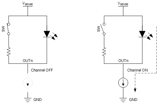
The device integrates an internal pullup circuit for LED diagnostics, shown in Figure 23. The circuit turns off during the channel on-state, but turns on to charge the output pin during the channel off-state. For an LED-short fault, both LSD1 and LSD2 are 1. For an LED-open fault, both LOD1 and LSD2 are 1. For an output short-to-GND fault, both LOD1 and LOD2 are 1. Table 5 shows the details.
 Figure 23. Internal Pullup Circuit
 Table 4. LOD-LSD Register Latch Timing
| GS COUNTER MODE | LOD1-LSD1 | LOD2-LSD2 |
|---|---|---|
| 12-bit | 9th GCLK rising edge | 4095th GCLK rising edge |
| 10-bit | 9th GCLK rising edge | 1023rd GCLK rising edge |
| 8-bit | 9th GCLK rising edge | 255th GCLK rising edge |
Table 5. LED Status Lookup Table
| LED STATUS | LOD-LSD RESULT | |||
|---|---|---|---|---|
| LOD1-LSD1 UPDATED AT 9th GCLK | LOD2-LSD2 UPDATED AT Nth GCLK(1) | |||
| LED Ok | LOD1 | 0 | LOD2 | 0 |
| LSD1 | 0 | LSD2 | 1 | |
| LED open | LOD1 | 1 | LOD2 | 0 |
| LSD1 | 0 | LSD2 | 1 | |
| LED short | LOD1 | 0 | LOD2 | 0 |
| LSD1 | 1 | LSD2 | 1 | |
| Output short-to-GND | LOD1 | 1 | LOD2 | 1 |
| LSD1 | 0 | LSD2 | 0 | |
In some cases, users may need to turn off output channels before the 9th GCLK to disable output channels, or turn on output channels at Nth GCLK to get more brightness. LOD_LSD faults are reported as shown in Table 6. Users can ignore the fault according to the GS register setting value.
Table 6. PWM Status Lookup Table
| LOD-LSD RESULT | ||||
|---|---|---|---|---|
| PWM STATUS | LOD1-LSD1 UPDATED AT 9th GCLK | LOD2-LSD2 UPDATED AT Nth GCLK(1) | ||
| PWM OK | LOD1 | 0 | LOD2 | 0 |
| LSD1 | 0 | LSD2 | 1 | |
| Channel off before 9th GCLK | LOD1 | 0 | LOD2 | 0 |
| LSD1 | 1 | LSD2 | 1 | |
| Channel on at Nth GCLK | LOD1 | 0 | LOD2 | 0 |
| LSD1 | 0 | LSD2 | 0 | |
The LOD_LSD status is updated every PWM cycle. Figure 14 is an example of the LOD-LSD register update timing for the 12-bit GS mode.