ZHCSK68B August   2019  – June 2022 TLIN1028-Q1

PRODUCTION DATA  

  1. 特性
  2. 应用
  3. 说明
  4. Revision History
  5. 说明(续)
  6. Pin Configuration and Functions
  7. Specifications
    1. 7.1 Absolute Maximum Ratings
    2. 7.2 ESD Ratings
    3. 7.3 ESD Ratings, IEC Specification
    4. 7.4 Recommended Operating Conditions
    5. 7.5 Thermal Information
    6. 7.6 Power Supply Characteristics
    7. 7.7 Electrical Charateristics
    8. 7.8 AC Switching Characteristics
    9. 7.9 Typical Characteristics
  8. Parameter Measurement Information
    1. 8.1 Test Circuit: Diagrams and Waveforms
  9. Detailed Description
    1. 9.1 Overview
    2. 9.2 Functional Block Diagram
    3. 9.3 Feature Description
      1. 9.3.1 LIN Pin
        1. 9.3.1.1 LIN Transmitter Characteristics
        2. 9.3.1.2 LIN Receiver Characteristics
          1. 9.3.1.2.1 Termination
      2. 9.3.2 TXD (Transmit Input)
      3. 9.3.3 RXD (Receive Output)
      4. 9.3.4 VSUP (Supply Voltage)
      5. 9.3.5 GND (Ground)
      6. 9.3.6 EN (Enable Input)
      7. 9.3.7 nRST (Reset Output)
      8. 9.3.8 VCC (Supply Output)
      9. 9.3.9 Protection Features
        1. 9.3.9.1 TXD Dominant Time Out (DTO)
        2. 9.3.9.2 Bus Stuck Dominant System Fault: False Wake Up Lockout
        3. 9.3.9.3 Thermal Shutdown
        4. 9.3.9.4 Under Voltage on VSUP
        5. 9.3.9.5 Unpowered Device and LIN Bus
    4. 9.4 Device Functional Modes
      1. 9.4.1 Normal Mode
      2. 9.4.2 Sleep Mode
      3. 9.4.3 Standby Mode
      4. 9.4.4 Wake-Up Events
        1. 9.4.4.1 Wake-Up Request (RXD)
      5. 9.4.5 Mode Transitions
      6. 9.4.6 Voltage Regulator
        1. 9.4.6.1 VCC
        2. 9.4.6.2 Output Capacitance Selection
        3. 9.4.6.3 Low-Voltage Tracking
        4. 9.4.6.4 Power Supply Recommendation
  10. 10Application and Implementation
    1. 10.1 Application Information
    2. 10.2 Typical Application
      1. 10.2.1 Design Requirements
        1. 10.2.1.1 Normal Mode Application Note
        2. 10.2.1.2 TXD Dominant State Timeout Application Note
        3. 10.2.1.3 Brownout
      2. 10.2.2 Detailed Design Procedures
      3. 10.2.3 Application Curves
  11. 11Power Supply Recommendations
  12. 12Layout
    1. 12.1 Layout Guidelines
    2. 12.2 Layout Example
  13. 13Device and Documentation Support
    1. 13.1 Documentation Support
      1. 13.1.1 Related Documentation
    2. 13.2 Related Links
    3. 13.3 接收文档更新通知
    4. 13.4 支持资源
    5. 13.5 Trademarks
    6. 13.6 Electrostatic Discharge Caution
    7. 13.7 术语表
  14. 14Mechanical, Packaging, and Orderable Information

封装选项

机械数据 (封装 | 引脚)
散热焊盘机械数据 (封装 | 引脚)
订购信息

Bus Stuck Dominant System Fault: False Wake Up Lockout

The device contains logic to detect bus stuck dominant system faults and prevents the device from waking up falsely during the system fault. Upon entering sleep mode, the device detects the state of the LIN bus. If the bus is dominant, the wake-up logic is locked out until a valid recessive on the bus “clears” the bus stuck dominant, preventing excessive current use. Figure 9-3 and Figure 9-4 show the behavior of this protection.
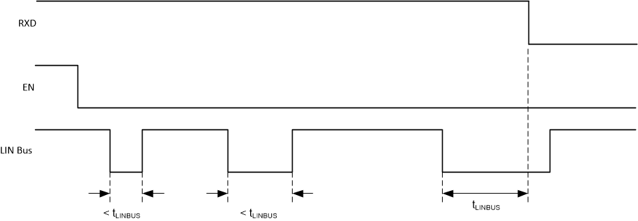
GUID-20201014-CA0I-LNXZ-HNSN-MBXMNZBRLQCQ-low.gifFigure 9-3 No Bus Fault: Entering Sleep Mode with Bus Recessive Condition and Wakeup
GUID-20201014-CA0I-BHVN-X6FS-ZZTM3Q8MXSHB-low.gifFigure 9-4 Bus Fault: Entering Sleep Mode with Bus Stuck Dominant Fault, Clearing, and Wakeup