-
TLV170x 2.2V 至 36V 微功耗比较器
封装选项
机械数据 (封装 | 引脚)
散热焊盘机械数据 (封装 | 引脚)
订购信息
TLV170x 2.2V 至 36V 微功耗比较器
1 特性
2 应用范围
- 过压和欠压检测器
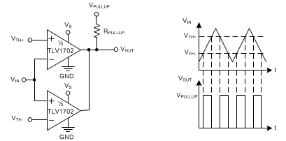
- 窗口比较器
- 过流检测器
- 零交叉检测器
- 针对以下应用的系统监控:
- 电源
- 白色家电
- 工业传感器
- 汽车
- 医疗
3 说明
TLV170x 系列器件提供宽电源范围、轨到轨输入、低静态电流和低传播延迟。 所有这些特性均符合行业标准,采用极小封装,借此,这些器件得以成为目前市场上可提供的最佳通用比较器。
集电极开路输出具有能够将输出拉至任意电压轨(最大可高出负电源 +36V)的优势,且不受 TLV170x 电源电压影响。
这些器件均可提供单通道 (TLV1701)、双通道 (TLV1702) 和四通道 (TLV1704) 三种版本。 低输入偏移电压、低输入偏置电流、低电源电流和开集配置使得 TLV170x 系列能够灵活处理从简单电压检测到驱动单个继电器的大多数应用。
所有器件的额定工作温度均在扩展的工业温度范围 –40°C 到 +125°C 内。
器件信息(1)
| 器件型号 | 封装 | 封装尺寸(标称值) |
|---|---|---|
| TLV1701 | SOT553 (5) | 1.20mm × 1.60mm |
| SC-70 (5) | 1.25mm × 2.00mm | |
| SOT-23 (5) | 1.60mm x 2.90mm | |
| TLV1702 | X2QFN (8) | 1.50mm x 1.50mm |
| VSSOP (8)(2) | 3.00mm × 3.00mm | |
| TLV1704 | TSSOP (14) | 4.40mm × 5.00mm |
- 要了解所有可用封装,请见数据表末尾的封装选项附录。
- VSSOP 封装与 MSOP 封装相同。
4 修订历史记录
Changes from C Revision (December 2014) to D Revision
Changes from B Revision (October 2014) to C Revision
- TLV1701 DCK 封装已从预览更改为量产数据Go
- Changed Handling Ratings table to ESD Ratings table, and moved storage temperature to Absolute Maximum Ratings tableGo
Changes from A Revision (September 2014) to B Revision
- 更改了器件信息表中的脚注 2:已将 TLV1701 添加到可用器件列表中Go
- Added TLV1701 to list of production data packages in footnote for the Pin Configuration and Functions section Go
- Added TLV1701 row to V(ESD) parameter in Handling Ratings tableGo
Changes from * Revision (December 2013) to A Revision
- 已将文档格式更改为符合最新的数据表标准;添加了新章节并移动了现有章节Go
- TLV1704 PW (TSSOP-14) 封装已从预览更改为量产数据Go
- 在集电极开路输出特性中添加了分项Go
- 在说明部分添加了第二段Go
- 已从说明部分中删除封装信息;冗余信息Go
- Changed Related Products table to Device Comparison table, moved from page 1, and added TLV370x familyGo
- Added TLV1701, TLV1702 RUG, and TLV704 package drawingsGo
- Added thermal information for TLV1702 RUG, TLV1704 PW, and all TLV1701 packagesGo
- Moved switching characteristics parameters from Electrical Characteristics table to new Switching Characteristics tableGo
- Changed all typical values in Switching Characteristics tableGo
- Changed title for Figure 1Go
- Changed Figure 8Go
- Changed Figure 9Go
- Changed Figure 10Go
- Changed Figure 11Go
- Changed Figure 12Go
- Changed Figure 13Go
- Changed Figure 14Go
- ChangedApplication Information and moved section Go
- Deleted Application Examples sectionGo
5 Device Comparison
| DEVICE | FEATURES |
|---|---|
| TLV3201 | 40-ns, 40-µA, push-pull comparator |
| TLV3202 | |
| TLV3501 | 4.5-ns, rail-to-rail, push-pull, high-speed comparator |
| TLV3502 | |
| TLV3401 | Nanopower open-drain output comparator |
| TLV3402 | |
| TLV3404 | |
| TLV3701 | Nanopower push-pull output comparator |
| TLV3702 | |
| TLV3704 | |
| REF3325 | 3.9-µA, SC70-3 voltage reference |
| REF3330 | |
| REF3333 |
6 Pin Configuration and Functions

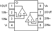
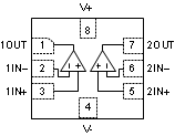
Pin Functions
| PIN | I/O | DESCRIPTION | |||
|---|---|---|---|---|---|
| NAME | NO. | ||||
| TLV1701 DBV, DCK, DRL |
TLV1702 DGK, RUG |
TLV1704 PW |
|||
| IN+ | 1 | — | — | I | Noninverting input |
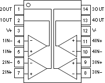
| 1IN+ | — | 3 | 5 | I | Noninverting input, channel 1 |
| 2IN+ | — | 5 | 7 | I | Noninverting input, channel 2 |
| 3IN+ | — | — | 9 | I | Noninverting input, channel 3 |
| 4IN+ | — | — | 11 | I | Noninverting input, channel 4 |
| IN– | 3 | — | — | I | Inverting input |
| 1IN– | — | 2 | 4 | I | Inverting input, channel 1 |
| 2IN– | — | 6 | 6 | I | Inverting input, channel 2 |
| 3IN– | — | — | 8 | I | Inverting input, channel 3 |
| 4IN– | — | — | 10 | I | Inverting input, channel 4 |
| OUT | 4 | — | — | O | Output |
| 1OUT | — | 1 | 2 | O | Output, channel 1 |
| 2OUT | — | 7 | 1 | O | Output, channel 2 |
| 3OUT | — | — | 14 | O | Output, channel 3 |
| 4OUT | — | — | 13 | O | Output, channel 4 |
| V+ | 5 | 8 | 3 | — | Positive (highest) power supply |
| V– | 2 | 4 | 12 | — | Negative (lowest) power supply |
7 Specifications
7.1 Absolute Maximum Ratings(1)
over operating free-air temperature range (unless otherwise noted)| MIN | MAX | UNIT | ||
|---|---|---|---|---|
| Supply voltage | +40 (±20) | V | ||
| Signal input pins | Voltage(2) | (VS–) – 0.5 | (VS+) + 0.5 | V |
| Current(2) | ±10 | mA | ||
| Output short-circuit(3) | Continuous | mA | ||
| Operating temperature range | –55 | +150 | °C | |
| Junction temperature, TJ | 150 | °C | ||
| Storage temperature, Tstg | –65 | +150 | °C | |
7.2 ESD Ratings
| VALUE | UNIT | |||
|---|---|---|---|---|
| TLV1701 and TLV1702 | ||||
| V(ESD) | Electrostatic discharge | Human-body model (HBM), per ANSI/ESDA/JEDEC JS-001(1) | ±2000 | V |
| Charged-device model (CDM), per JEDEC specification JESD22-C101(2) | ±1500 | |||
| TLV1704 | ||||
| V(ESD) | Electrostatic discharge | Human-body model (HBM), per ANSI/ESDA/JEDEC JS-001(1) | ±1000 | V |
| Charged-device model (CDM), per JEDEC specification JESD22-C101(2) | ±1500 | |||
7.3 Recommended Operating Conditions
over operating free-air temperature range (unless otherwise noted)| MIN | NOM | MAX | UNIT | ||
|---|---|---|---|---|---|
| Supply voltage VS = (VS+) – (VS–) | 2.2 (±1.1) | 36 (±18) | V | ||
| Specified temperature | –40 | 125 | °C | ||
7.4 Thermal Information: TLV1701
| THERMAL METRIC(1) | TLV1701 | UNIT | |||
|---|---|---|---|---|---|
| DRL (SOT553) | DCK (SC70) | DBV (SOT23) | |||
| 5 PINS | 5 PINS | 5 PINS | |||
| RθJA | Junction-to-ambient thermal resistance | 271.5 | 283.6 | 233.1 | °C/W |
| RθJC(top) | Junction-to-case (top) thermal resistance | 115.6 | 94.1 | 156.4 | °C/W |
| RθJB | Junction-to-board thermal resistance | 89.7 | 61.3 | 60.6 | °C/W |
| ψJT | Junction-to-top characterization parameter | 17.6 | 1.9 | 35.7 | °C/W |
| ψJB | Junction-to-board characterization parameter | 89.2 | 60.5 | 59.7 | °C/W |
| RθJC(bot) | Junction-to-case (bottom) thermal resistance | N/A | N/A | N/A | °C/W |
7.5 Thermal Information: TLV1702 and TLV1704
| THERMAL METRIC(1) | TLV1702 | TLV1704 | UNIT | ||
|---|---|---|---|---|---|
| RUG (QFN) | DGK (VSSOP) | PW (TSSOP) | |||
| 8 PINS | 8 PINS | 14 PINS | |||
| θJA | Junction-to-ambient thermal resistance | 205.6 | 199 | 128.1 | °C/W |
| θJCtop | Junction-to-case (top) thermal resistance | 77.1 | 89.5 | 56.5 | °C/W |
| θJB | Junction-to-board thermal resistance | 107.0 | 120.4 | 69.9 | °C/W |
| ψJT | Junction-to-top characterization parameter | 2.0 | 22.0 | 9.1 | °C/W |
| ψJB | Junction-to-board characterization parameter | 107.0 | 118.7 | 69.3 | °C/W |
| θJCbot | Junction-to-case (bottom) thermal resistance | N/A | N/A | N/A | °C/W |
7.6 Electrical Characteristics
at TA = +25°C, VS = +2.2 V to +36 V, CL = 15 pF, RPULLUP = 5.1 kΩ, VCM = VS / 2, and VS = VPULLUP (unless otherwise noted)| PARAMETER | TEST CONDITIONS | MIN | TYP | MAX | UNIT | ||
|---|---|---|---|---|---|---|---|
| OFFSET VOLTAGE | |||||||
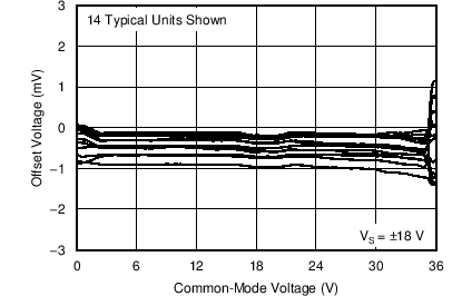
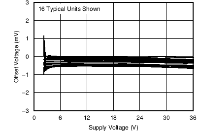
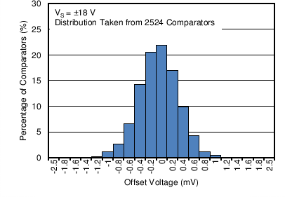
| VOS | Input offset voltage | TA = 25°C, VS = 2.2 V | ±0.5 | ±3.5 | mV | ||
| TA = 25°C, VS = 36 V | ±0.3 | ±2.5 | mV | ||||
| TA = –40°C to +125°C | ±5.5 | mV | |||||
| dVOS/dT | Input offset voltage drift | TA = –40°C to +125°C | ±4 | ±20 | μV/°C | ||
| PSRR | Power-supply rejection ratio | 15 | 100 | μV/V | |||
| TA = –40°C to +125°C | 20 | μV/V | |||||
| INPUT VOLTAGE RANGE | |||||||
| VCM | Common-mode voltage range | TA = –40°C to +125°C | (V–) | (V+) | V | ||
| INPUT BIAS CURRENT | |||||||
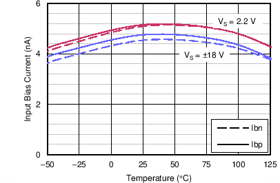
| IB | Input bias current | 5 | 15 | nA | |||
| TA = –40°C to +125°C | 20 | nA | |||||
| IOS | Input offset current | 0.5 | nA | ||||
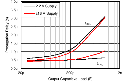
| CLOAD | Capacitive load drive | See Typical Characteristics | |||||
| OUTPUT | |||||||
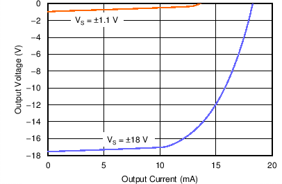
| VO | Voltage output swing from rail | IO ≤ 4 mA, input overdrive = 100 mV, VS = 36 V |
900 | mV | |||
| IO = 0 mA, input overdrive = 100 mV, VS = 36 V |
600 | mV | |||||
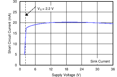
| ISC | Short circuit sink current | 20 | mA | ||||
| Output leakage current | VIN+ > VIN– | 70 | nA | ||||
| POWER SUPPLY | |||||||
| VS | Specified voltage range | 2.2 | 36 | V | |||
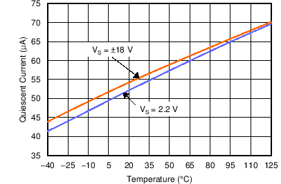
| IQ | Quiescent current (per channel) | IO = 0 A | 55 | 75 | μA | ||
| IO = 0 A, TA = –40°C to +125°C | 100 | μA | |||||
7.7 Switching Characteristics
at TA = +25°C, VS = +2.2 V to +36 V, CL = 15 pF, RPULLUP = 5.1 kΩ, VCM = VS / 2, and VS = VPULLUP (unless otherwise noted)| PARAMETER | TEST CONDITIONS | MIN | TYP | MAX | UNIT | |
|---|---|---|---|---|---|---|
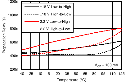
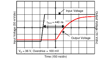
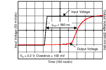
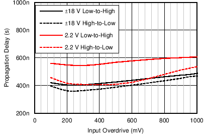
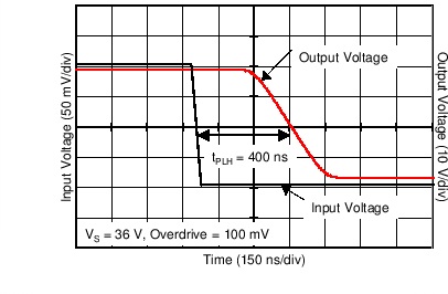
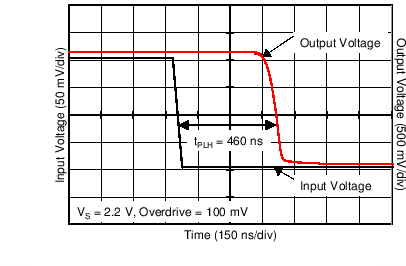
| tpHL | Propagation delay time, high-to-low | Input overdrive = 100 mV | 460 | ns | ||
| tpLH | Propagation delay time, low-to-high | Input overdrive = 100 mV | 560 | ns | ||
| tR | Rise time | Input overdrive = 100 mV | 365 | ns | ||
| tF | Fall time | Input overdrive = 100 mV | 240 | ns | ||
7.8 Typical Characteristics
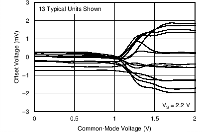
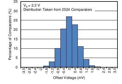
at TA = +25°C, VS = +5 V, RPULLUP = 5.1 kΩ, and input overdrive = 100 mV (unless otherwise noted)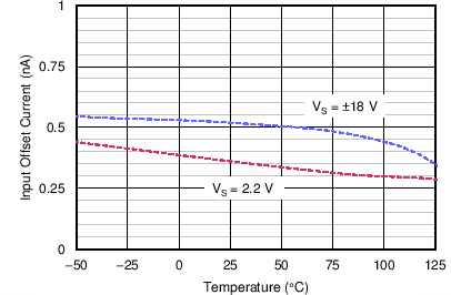
8 Detailed Description
8.1 Overview
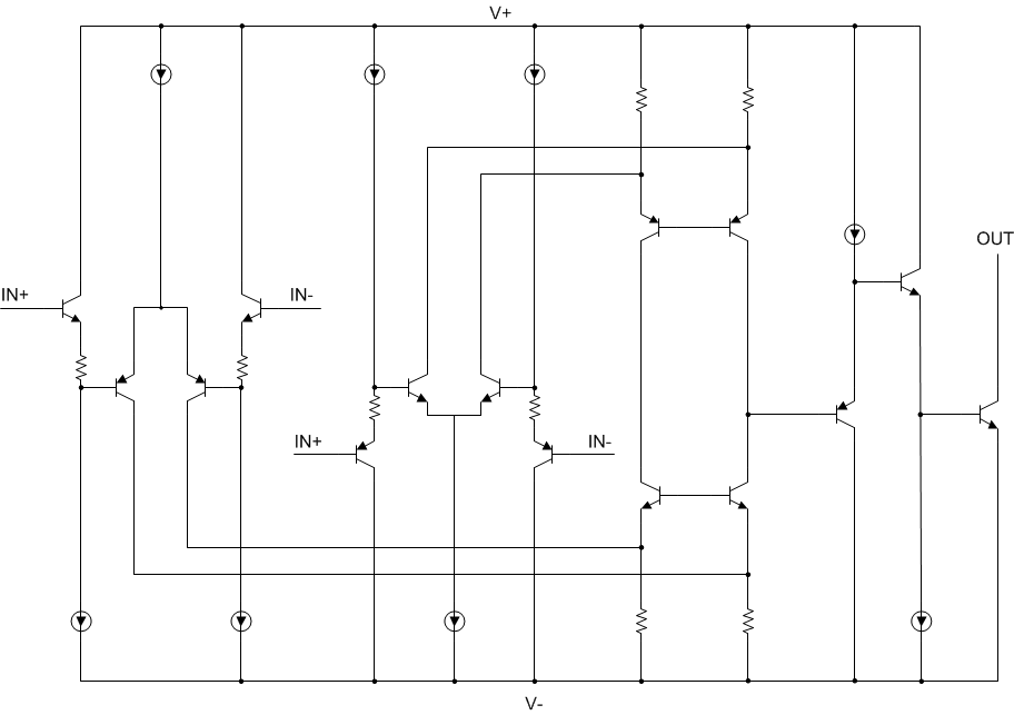
The TLV170x comparators features rail-to-rail input and output on supply voltages as high as 36 V. The rail-to-rail input stage enables detection of signals close to the supply and ground. The open collector configuration allows the device to be used in wired-OR configurations, such as a window comparator. A low supply current of 55 μA per channel with small, space-saving packages, makes these comparators versatile for use in a wide range of applications, from portable to industrial.
8.2 Functional Block Diagram
8.3 Feature Description
8.3.1 Comparator Inputs
The TLV170x are rail-to-rail input comparators, with an input common-mode range that includes the supply rails. The TLV170x is designed to prevent phase inversion when the input pins exceed the supply voltage. Figure 18 shows the TLV170x response when input voltages exceed the supply, resulting in no phase inversion.
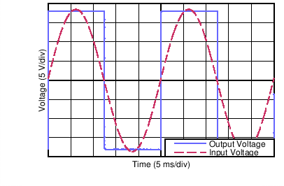 Figure 18. No Phase Inversion: Comparator Response to Input Voltage
(Propagation Delay Included)
