SBOS858 April 2017 TLV171-Q1
PRODUCTION DATA.
1 Features
- Qualified for Automotive Applications
- AEC-Q100 Test Guidance With the Following Results:
- Device Temperature Grade 1:
–40°C to +125°C Ambient Operating Temperature - Device HBM ESD Classification Level:
- Level 3A for TLV171-Q1 and TLV2171-Q1
- Level 2 for TLV4171-Q1
- Device CDM ESD Classification Level
- Level C4A for TLV171-Q1
- Level C6 for TLV2171-Q1and TLV4171-Q1
- Device Temperature Grade 1:
- Supply Range:
- Single-Supply: 4.5 V to 36 V
- Dual-Supply ±2.25 V to ±18 V
- Low Noise: 16 nV/√Hz at 1 kHz
- Low Offset Drift: ±1 µV/°C (Typical)
- Input Range Includes Negative Supply
- Input Range Operates to Positive Supply With Reduced Performance
- Rail-to-Rail Output
- Gain Bandwidth: 3 MHz
- Low Quiescent Current: 525 µA per Amplifier
- Common-Mode Rejection: 120 dB (Typical)
- Low Input Bias Current: 10 pA
2 Applications
- Automotive
- ADAS
- Body Electronics
- Lighting
- Current Sensing
- Power Train
3 Description
The TLVx171-Q1 family of devices is a 36-V,
single-supply, low-noise operational amplifier (op amp) with the ability to operate on supplies ranging from 4.5 V (± 2.25 V) to 36 V (±18 V). This series is available in multiple packages and offers low offset, drift, and low quiescent current. The single, dual, and quad versions all have identical specifications for maximum design flexibility.
Device Information(1)
| PART NUMBER | PACKAGE | BODY SIZE (NOM) |
|---|---|---|
| TLV171-Q1 | SOT-23 (5) | 2.90 mm × 1.60 mm |
| TLV2171-Q1 | SOIC (8) | 4.90 mm × 3.91 mm |
| VSSOP (8) | 3.00 mm × 3.00 mm | |
| TLV4171-Q1 | SOIC (14) | 8.65 mm × 3.91 mm |
| TSSOP (14) | 5.00 mm × 4.40 mm |
- For all available packages, see the orderable addendum at the end of the data sheet.
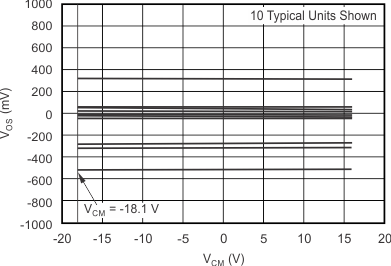
Offset Voltage vs Common-Mode Voltage: VSUPPLY = ±18 V

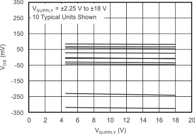
Offset Voltage vs Power Supply
