SBOS858 April 2017 TLV171-Q1
PRODUCTION DATA.
8 Application and Implementation
NOTE
Information in the following applications sections is not part of the TI component specification, and TI does not warrant its accuracy or completeness. TI’s customers are responsible for determining suitability of components for their purposes. Customers should validate and test their design implementation to confirm system functionality.
8.1 Application Information
The TLV171-Q1 operational amplifier family provides high overall performance, making the device ideal for many general-purpose applications. The excellent offset drift of only 1 µV/°C provides excellent stability over the entire temperature range. In addition, the device offers very good overall performance with high CMRR, PSRR, and AOL. As with all amplifiers, applications with noisy or high-impedance power supplies require decoupling capacitors close to the device pins. In most cases, 0.1-µF capacitors are adequate.
8.1.1 Electrical Overstress
Designers often ask questions about the capability of an op amp to withstand electrical overstress. These questions tend to focus on the device inputs, but may involve the supply voltage pins or even the output pin. Each of these different pin functions have electrical stress limits determined by the voltage breakdown characteristics of the particular semiconductor fabrication process and specific circuits connected to the pin. Additionally, internal electrostatic discharge (ESD) protection is built into these circuits to protect them from accidental ESD events both before and during product assembly.
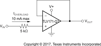
These ESD protection diodes also provide in-circuit, input overdrive protection, as long as the current is limited to 10 mA as stated in Absolute Maximum Ratings. Figure 29 shows how a series input resistor can be added to the input to limit the input current. The added resistor contributes thermal noise at the amplifier input and its value must be kept to a minimum in noise-sensitive applications.
 Figure 29. Input Current Protection
An ESD event produces a short duration, high-voltage pulse that is transformed into a short duration, high-current pulse as it discharges through a semiconductor device. The ESD protection circuits are designed to provide a current path around the operational amplifier core to prevent it from being damaged. The energy absorbed by the protection circuitry is then dissipated as heat.
When the operational amplifier connects into a circuit, the ESD protection components are intended to remain inactive and not become involved in the application circuit operation. However, circumstances may arise where an applied voltage exceeds the operating voltage range of a given pin. If this condition occurs, there is a risk that some of the internal ESD protection circuits may be biased on, and conduct current. Any such current flow occurs through ESD cells and rarely involves the absorption device.
If the ability of the supply to absorb this current is uncertain, external zener diodes may be added to the supply pins. The zener voltage must be selected such that the diode does not turn on during normal operation.
However, the zener voltage must be low enough so that the zener diode conducts if the supply pin begins to rise above the safe operating supply voltage level.
8.2 Typical Application
8.2.1 Capacitive Load Drive Solution Using an Isolation Resistor
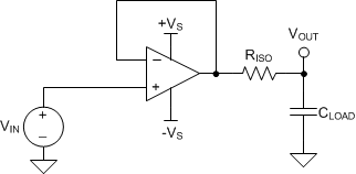
The TLVx171-Q1 device can be used capacitive loads such as cable shields, reference buffers, MOSFET gates, and diodes. The circuit uses an isolation resistor (RISO) to stabilize the output of an op amp. RISO modifies the open loop gain of the system to ensure the circuit has sufficient phase margin.
 Figure 30. Unity-Gain Buffer with RISO Stability Compensation
8.2.1.1 Design Requirements
The design requirements are:
- Supply voltage: 30 V (±15 V)
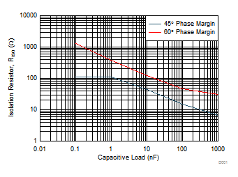
- Capacitive loads: 100 pF, 1000 pF, 0.01 μF, 0.1 μF, and 1 μF
- Phase margin: 45° and 60°
8.2.1.2 Detailed Design Procedure
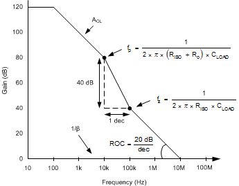
Figure 31 shows a unity-gain buffer driving a capacitive load. Equation 1 shows the transfer function for the circuit in Figure 31. Not shown in Figure 31 is the open-loop output resistance of the op amp, Ro.

The transfer function in Equation 1 has a pole and a zero. The frequency of the pole (fp) is determined by (Ro + RISO) and CLOAD. Components RISO and CLOAD determine the frequency of the zero (fz). A stable system is obtained by selecting RISO such that the rate of closure (ROC) between the open-loop gain (AOL) and 1/β is 20 dB/decade. Figure 31 shows the concept. The 1/β curve for a unity-gain buffer is 0 dB.
 Figure 31. Unity-Gain Amplifier with RISO Compensation
ROC stability analysis is typically simulated. The validity of the analysis depends on multiple factors, especially the accurate modeling of Ro. In addition to simulating the ROC, a robust stability analysis includes a measurement of overshoot percentage and AC gain peaking of the circuit using a function generator, oscilloscope, and gain and phase analyzer. Phase margin is then calculated from these measurements. Table 4 lists the overshoot percentage and AC gain peaking that correspond to phase margins of 45° and 60°. For more details on this design and other alternative devices that can be used in place of the TLVx171-Q1, see Capacitive Load Drive Solution using an Isolation Resistor.
Table 4. Phase Margin versus Overshoot and AC Gain Peaking
| PHASE MARGIN | OVERSHOOT | AC GAIN PEAKING |
|---|---|---|
| 45° | 23.3% | 2.35 dB |
| 60° | 8.8% | 0.28 dB |
