ZHCSJ63 December   2018 TLV1805

PRODUCTION DATA.  

  1. 特性
  2. 应用
  3. 说明
    1.     Device Images
      1.      采用 P 沟道 MOSFET 的过压保护
      2.      采用 P 沟道 MOSFET 的反向电流和过压保护
  4. 修订历史记录
  5. 说明 (续)
  6. Pin Configuration and Functions
    1.     Pin Functions
  7. Specifications
    1. 7.1 Absolute Maximum Ratings
    2. 7.2 ESD Ratings
    3. 7.3 Recommended Operating Conditions
    4. 7.4 Thermal Information
    5. 7.5 Electrical Characteristics
    6. 7.6 Switching Characteristics
    7. 7.7 Typical Characteristics
  8. Detailed Description
    1. 8.1 Overview
    2. 8.2 Functional Block Diagram
    3. 8.3 Feature Description
      1. 8.3.1 Rail to Rail Inputs
      2. 8.3.2 Power On Reset
      3. 8.3.3 High Power Push-Pull Output
      4. 8.3.4 Shutdown Function
      5. 8.3.5 Internal Hysteresis
    4. 8.4 Device Functional Modes
      1. 8.4.1 External Hysteresis
        1. 8.4.1.1 Inverting Comparator With Hysteresis
        2. 8.4.1.2 Noninverting Comparator With Hysteresis
  9. Application and Implementation
    1. 9.1 Application Information
    2. 9.2 Typical Applications
      1. 9.2.1 Design Requirements
      2. 9.2.2 Detailed Design Procedure
      3. 9.2.3 Application Curve
      4. 9.2.4 Reverse Current Protection Using MOSFET and TLV1805
        1. 9.2.4.1 Minimum Reverse Current
        2. 9.2.4.2 N-Channel Reverse Current Protection Circuit
          1. 9.2.4.2.1 N-Channel Oscillator Circuit
      5. 9.2.5 P-Channel Reverse Current Protection Circuit
      6. 9.2.6 P-Channel Reverse Current Protection With Overvotlage Protection
      7. 9.2.7 ORing MOSFET Controller
  10. 10Power Supply Recommendations
  11. 11Layout
    1. 11.1 Layout Guidelines
    2. 11.2 Layout Example
  12. 12器件和文档支持
    1. 12.1 文档支持
      1. 12.1.1 相关文档
    2. 12.2 接收文档更新通知
    3. 12.3 社区资源
    4. 12.4 商标
    5. 12.5 静电放电警告
    6. 12.6 术语表
  13. 13机械、封装和可订购信息

封装选项

机械数据 (封装 | 引脚)
散热焊盘机械数据 (封装 | 引脚)
订购信息

Internal Hysteresis

The TLV1805 contains 14mV of internal hysteresis.

The hysteresis transfer curve is shown in Figure 63. This curve is a function of three components: VTH, VOS, and VHYST:

  • VTH is the actual set voltage or threshold trip voltage.
  • VOS is the internal offset voltage between VIN+ and VIN–. This voltage is added to VTH to form the actual trip point at which the comparator must respond to change output states.
  • VHYST is the internal hysteresis (or trip window) that is designed to reduce comparator sensitivity to noise
    (14 mV for the TLV1805).
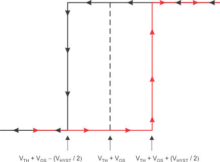
TLV1805 ai_hyst_transfer_bos694.gifFigure 63. Hysteresis Transfer Curve