ZHCSJ63 December   2018 TLV1805

PRODUCTION DATA.  

  1. 特性
  2. 应用
  3. 说明
    1.     Device Images
      1.      采用 P 沟道 MOSFET 的过压保护
      2.      采用 P 沟道 MOSFET 的反向电流和过压保护
  4. 修订历史记录
  5. 说明 (续)
  6. Pin Configuration and Functions
    1.     Pin Functions
  7. Specifications
    1. 7.1 Absolute Maximum Ratings
    2. 7.2 ESD Ratings
    3. 7.3 Recommended Operating Conditions
    4. 7.4 Thermal Information
    5. 7.5 Electrical Characteristics
    6. 7.6 Switching Characteristics
    7. 7.7 Typical Characteristics
  8. Detailed Description
    1. 8.1 Overview
    2. 8.2 Functional Block Diagram
    3. 8.3 Feature Description
      1. 8.3.1 Rail to Rail Inputs
      2. 8.3.2 Power On Reset
      3. 8.3.3 High Power Push-Pull Output
      4. 8.3.4 Shutdown Function
      5. 8.3.5 Internal Hysteresis
    4. 8.4 Device Functional Modes
      1. 8.4.1 External Hysteresis
        1. 8.4.1.1 Inverting Comparator With Hysteresis
        2. 8.4.1.2 Noninverting Comparator With Hysteresis
  9. Application and Implementation
    1. 9.1 Application Information
    2. 9.2 Typical Applications
      1. 9.2.1 Design Requirements
      2. 9.2.2 Detailed Design Procedure
      3. 9.2.3 Application Curve
      4. 9.2.4 Reverse Current Protection Using MOSFET and TLV1805
        1. 9.2.4.1 Minimum Reverse Current
        2. 9.2.4.2 N-Channel Reverse Current Protection Circuit
          1. 9.2.4.2.1 N-Channel Oscillator Circuit
      5. 9.2.5 P-Channel Reverse Current Protection Circuit
      6. 9.2.6 P-Channel Reverse Current Protection With Overvotlage Protection
      7. 9.2.7 ORing MOSFET Controller
  10. 10Power Supply Recommendations
  11. 11Layout
    1. 11.1 Layout Guidelines
    2. 11.2 Layout Example
  12. 12器件和文档支持
    1. 12.1 文档支持
      1. 12.1.1 相关文档
    2. 12.2 接收文档更新通知
    3. 12.3 社区资源
    4. 12.4 商标
    5. 12.5 静电放电警告
    6. 12.6 术语表
  13. 13机械、封装和可订购信息

封装选项

机械数据 (封装 | 引脚)
散热焊盘机械数据 (封装 | 引脚)
订购信息

Noninverting Comparator With Hysteresis

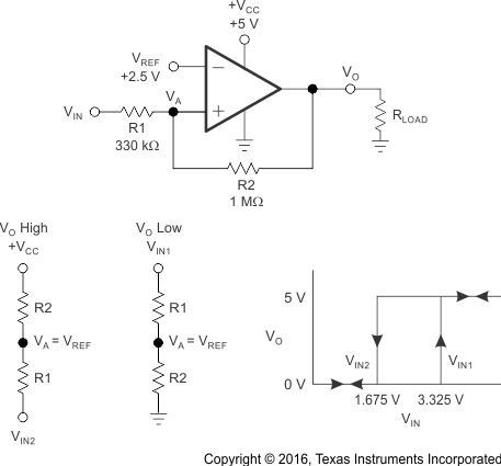
TLV1805 ai_noninverting_bos561.gifFigure 65. TLV1805-Q1 in a Noninverting Configuration With Hysteresis

A noninverting comparator with hysteresis requires a two-resistor network, as shown in Figure 65, and a voltage reference (VREF) at the inverting input. When VIN is low, the output is also low. For the output to switch from low to high, VIN must rise to VIN1. Use Equation 4 to calculate VIN1.

Equation 4. TLV1805 q_vin1_bos694.gif

When VIN is high, the output is also high. For the comparator to switch back to a low state, VIN must drop to VIN2 such that VA is equal to VREF. Use Equation 5 to calculate VIN2.

Equation 5. TLV1805 q_vin2_bos561.gif

The hysteresis of this circuit is the difference between VIN1 and VIN2, as shown in Equation 6.

Equation 6. TLV1805 q_delta_vin_bos561.gif