ZHCSJ63 December   2018 TLV1805

PRODUCTION DATA.  

  1. 特性
  2. 应用
  3. 说明
    1.     Device Images
      1.      采用 P 沟道 MOSFET 的过压保护
      2.      采用 P 沟道 MOSFET 的反向电流和过压保护
  4. 修订历史记录
  5. 说明 (续)
  6. Pin Configuration and Functions
    1.     Pin Functions
  7. Specifications
    1. 7.1 Absolute Maximum Ratings
    2. 7.2 ESD Ratings
    3. 7.3 Recommended Operating Conditions
    4. 7.4 Thermal Information
    5. 7.5 Electrical Characteristics
    6. 7.6 Switching Characteristics
    7. 7.7 Typical Characteristics
  8. Detailed Description
    1. 8.1 Overview
    2. 8.2 Functional Block Diagram
    3. 8.3 Feature Description
      1. 8.3.1 Rail to Rail Inputs
      2. 8.3.2 Power On Reset
      3. 8.3.3 High Power Push-Pull Output
      4. 8.3.4 Shutdown Function
      5. 8.3.5 Internal Hysteresis
    4. 8.4 Device Functional Modes
      1. 8.4.1 External Hysteresis
        1. 8.4.1.1 Inverting Comparator With Hysteresis
        2. 8.4.1.2 Noninverting Comparator With Hysteresis
  9. Application and Implementation
    1. 9.1 Application Information
    2. 9.2 Typical Applications
      1. 9.2.1 Design Requirements
      2. 9.2.2 Detailed Design Procedure
      3. 9.2.3 Application Curve
      4. 9.2.4 Reverse Current Protection Using MOSFET and TLV1805
        1. 9.2.4.1 Minimum Reverse Current
        2. 9.2.4.2 N-Channel Reverse Current Protection Circuit
          1. 9.2.4.2.1 N-Channel Oscillator Circuit
      5. 9.2.5 P-Channel Reverse Current Protection Circuit
      6. 9.2.6 P-Channel Reverse Current Protection With Overvotlage Protection
      7. 9.2.7 ORing MOSFET Controller
  10. 10Power Supply Recommendations
  11. 11Layout
    1. 11.1 Layout Guidelines
    2. 11.2 Layout Example
  12. 12器件和文档支持
    1. 12.1 文档支持
      1. 12.1.1 相关文档
    2. 12.2 接收文档更新通知
    3. 12.3 社区资源
    4. 12.4 商标
    5. 12.5 静电放电警告
    6. 12.6 术语表
  13. 13机械、封装和可订购信息

封装选项

机械数据 (封装 | 引脚)
散热焊盘机械数据 (封装 | 引脚)
订购信息

Pin Configuration and Functions

TLV1805 DBV Package
6-Pin SOT-23
Top View
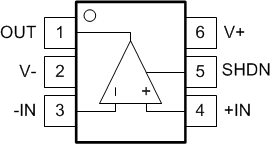
TLV1805 SOT391_wSD.gif
Note the reversed positions of the input pins. This differs from a similar popular pinout.

Pin Functions

PIN TYPE DESCRIPTION
NAME NO.
IN+ 4 I Noninverting input
IN– 3 I Inverting input
OUT 1 O Output
SHDN 5 I Shutdown (active high)
V+ 6 P Positive (highest) power supply
V– 2 P Negative (lowest) power supply