ZHCSLZ2B October   2022  – September 2023 TLV1811-Q1 , TLV1812-Q1 , TLV1814-Q1 , TLV1821-Q1 , TLV1822-Q1 , TLV1824-Q1

PRODMIX  

  1.   1
  2. 特性
  3. 应用
  4. 说明
  5. Revision History
  6. Pin Configuration and Functions
    1.     Pin Functions: TLV18x1-Q1 and TLV18x1L-Q1
    2.     Pin Functions: TLV1812-Q1 and TLV1822-Q1
    3.     Pin Functions: TLV1814-Q1 and TLV1824-Q1
  7. Specifications
    1. 6.1 Absolute Maximum Ratings
    2. 6.2 ESD Ratings
    3. 6.3 Recommended Operating Conditions
    4. 6.4 Thermal Information - Single
    5. 6.5 Thermal Information - Dual
    6. 6.6 Thermal Information - Quad
    7. 6.7 Electrical Characteristics
    8. 6.8 Switching Characteristics
  8. Typical Characteristics
  9. Detailed Description
    1. 8.1 Overview
    2. 8.2 Functional Block Diagrams
    3. 8.3 Feature Description
    4. 8.4 Device Functional Modes
      1. 8.4.1 Inputs
        1. 8.4.1.1 TLV18xx Rail-to-Rail Input
        2. 8.4.1.2 ESD Protection
        3. 8.4.1.3 Unused Inputs
      2. 8.4.2 Outputs
        1. 8.4.2.1 TLV181x-Q1 Push-Pull Output
        2. 8.4.2.2 TLV182x-Q1 Open-Drain Output
      3. 8.4.3 Power-On Reset (POR)
      4. 8.4.4 Hysteresis
  10. Application and Implementation
    1. 9.1 Application Information
      1. 9.1.1 Basic Comparator Definitions
        1. 9.1.1.1 Operation
        2. 9.1.1.2 Propagation Delay
        3. 9.1.1.3 Overdrive Voltage
      2. 9.1.2 Hysteresis
        1. 9.1.2.1 Inverting Comparator With Hysteresis
        2. 9.1.2.2 Non-Inverting Comparator With Hysteresis
        3. 9.1.2.3 Inverting and Non-Inverting Hysteresis using Open-Drain Output
    2. 9.2 Typical Applications
      1. 9.2.1 Window Comparator
        1. 9.2.1.1 Design Requirements
        2. 9.2.1.2 Detailed Design Procedure
        3. 9.2.1.3 Application Curve
      2. 9.2.2 Square-Wave Oscillator
        1. 9.2.2.1 Design Requirements
        2. 9.2.2.2 Detailed Design Procedure
        3. 9.2.2.3 Application Curve
      3. 9.2.3 Adjustable Pulse Width Generator
      4. 9.2.4 Time Delay Generator
      5. 9.2.5 Logic Level Shifter
      6. 9.2.6 One-Shot Multivibrator
      7. 9.2.7 Bi-Stable Multivibrator
      8. 9.2.8 Zero Crossing Detector
      9. 9.2.9 Pulse Slicer
    3. 9.3 Power Supply Recommendations
    4. 9.4 Layout
      1. 9.4.1 Layout Guidelines
      2. 9.4.2 Layout Example
  11. 10Device and Documentation Support
    1. 10.1 Documentation Support
      1. 10.1.1 Related Documentation
    2. 10.2 接收文档更新通知
    3. 10.3 支持资源
    4. 10.4 Trademarks
    5. 10.5 静电放电警告
    6. 10.6 术语表
  12. 11Mechanical, Packaging, and Orderable Information

封装选项

机械数据 (封装 | 引脚)
散热焊盘机械数据 (封装 | 引脚)
订购信息

Hysteresis

The basic comparator configuration may oscillate or produce a noisy "chatter" output if the applied differential input voltage is near the comparator's offset voltage. This usually occurs when the input signal is moving very slowly across the switching threshold of the comparator.

This problem can be prevented by the addition of hysteresis or positive feedback.

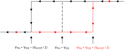
The hysteresis transfer curve is shown in Figure 9-2. This curve is a function of three components: VTH, VOS, and VHYST:

  • VTH is the actual set voltage or threshold trip voltage.
  • VOS is the internal offset voltage between VIN+ and VIN–. This voltage is added to VTH to form the actual trip point at which the comparator must respond to change output states.
  • VHYST is the hysteresis (or trip window) that is designed to reduce comparator sensitivity to noise.
GUID-D9090988-BB9B-46F7-8A02-4A1EE821C44D-low.gif
Figure 9-2 Hysteresis Transfer Curve

For more information, please see Application Note SBOA219 "Comparator with and without hysteresis circuit".