ZHCSLV0C September   2022  – September 2023 TLV1811 , TLV1812 , TLV1814 , TLV1821 , TLV1822 , TLV1824

PRODMIX  

  1.   1
  2. 特性
  3. 应用
  4. 说明
  5. Revision History
  6. Pin Configuration and Functions
    1.     Pin Functions: TLV18x1 and TLV18x1L
    2.     Pin Functions: TLV1812 and TLV1822
    3.     Pin Functions: TLV1814 and TLV1824
  7. Specifications
    1. 6.1 Absolute Maximum Ratings
    2. 6.2 ESD Ratings
    3. 6.3 Recommended Operating Conditions
    4. 6.4 Thermal Information - Single
    5. 6.5 Thermal Information - Dual
    6. 6.6 Thermal Information - Quad
    7. 6.7 Electrical Characteristics
    8. 6.8 Switching Characteristics
  8. Typical Characteristics
  9. Detailed Description
    1. 8.1 Overview
    2. 8.2 Functional Block Diagrams
    3. 8.3 Feature Description
    4. 8.4 Device Functional Modes
      1. 8.4.1 Inputs
        1. 8.4.1.1 TLV18xx Rail-to-Rail Input
        2. 8.4.1.2 ESD Protection
        3. 8.4.1.3 Unused Inputs
      2. 8.4.2 Outputs
        1. 8.4.2.1 TLV181x Push-Pull Output
        2. 8.4.2.2 TLV182x Open-Drain Output
      3. 8.4.3 Power-On Reset (POR)
      4. 8.4.4 Hysteresis
  10. Application and Implementation
    1. 9.1 Application Information
      1. 9.1.1 Basic Comparator Definitions
        1. 9.1.1.1 Operation
        2. 9.1.1.2 Propagation Delay
        3. 9.1.1.3 Overdrive Voltage
      2. 9.1.2 Hysteresis
        1. 9.1.2.1 Inverting Comparator With Hysteresis
        2. 9.1.2.2 Non-Inverting Comparator With Hysteresis
        3. 9.1.2.3 Inverting and Non-Inverting Hysteresis using Open-Drain Output
    2. 9.2 Typical Applications
      1. 9.2.1 Window Comparator
        1. 9.2.1.1 Design Requirements
        2. 9.2.1.2 Detailed Design Procedure
        3. 9.2.1.3 Application Curve
      2. 9.2.2 Square-Wave Oscillator
        1. 9.2.2.1 Design Requirements
        2. 9.2.2.2 Detailed Design Procedure
        3. 9.2.2.3 Application Curve
      3. 9.2.3 Adjustable Pulse Width Generator
      4. 9.2.4 Time Delay Generator
      5. 9.2.5 Logic Level Shifter
      6. 9.2.6 One-Shot Multivibrator
      7. 9.2.7 Bi-Stable Multivibrator
      8. 9.2.8 Zero Crossing Detector
      9. 9.2.9 Pulse Slicer
    3. 9.3 Power Supply Recommendations
    4. 9.4 Layout
      1. 9.4.1 Layout Guidelines
      2. 9.4.2 Layout Example
  11. 10Device and Documentation Support
    1. 10.1 Documentation Support
      1. 10.1.1 Related Documentation
    2. 10.2 接收文档更新通知
    3. 10.3 支持资源
    4. 10.4 Trademarks
    5. 10.5 静电放电警告
    6. 10.6 术语表
  12. 11Mechanical, Packaging, and Orderable Information

封装选项

机械数据 (封装 | 引脚)
散热焊盘机械数据 (封装 | 引脚)
订购信息

Pulse Slicer

A Pulse Slicer is a variation of the Zero Crossing Detector and is used to detect the zero crossings on an input signal with a varying baseline level. This circuit works best with symmetrical waveforms. The RC network of R1 and C1 establishes an mean reference voltage VREF, which tracks the mean amplitude of the VIN signal. The non-inverting input is directly connected to VREF through R2. R2 and R3 are used to produce hysteresis to keep transitions free of spurious toggles. The time constant is a tradeoff between long-term symmetry and response time to changes in amplitude.

If the waveform is data, it is recommended that the data be encoded in NRZ (Non-Return to Zero) format to maintain proper average baseline. Asymmetrical inputs may suffer from timing distortions caused by the changing VREF average voltage.
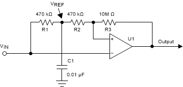
GUID-38218F92-47FC-4F40-869A-03CDEB104412-low.gifFigure 9-18 Pulse Slicer

For this design, follow these design requirements:

  • The RC constant value (R2 and C1) must support the targeted data rate to maintain a valid tripping threshold.
  • The hysteresis introduced with R2 and R43 helps to avoid spurious output toggles.

The TLV182x may also be used, but with the addition of a pull-up resistor on the output (not shown for clarity).

Figure 9-19 shows the results of a 9600 baud data signal riding on a varying baseline.
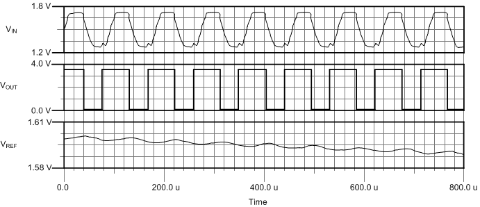
GUID-52123FBA-59FB-48ED-9329-B66EAE456E66-low.gifFigure 9-19 Pulse Slicer Waveforms