SNOSDG6 September 2024 TLV1831-Q1
ADVANCE INFORMATION
- 1
- 1 Features
- 2 Applications
- 3 Description
- 4 Pin Configuration and Functions
- 5 Specifications
- 6 Detailed Description
- 7 Application and Implementation
- 8 Device and Documentation Support
- 9 Revision History
- 10Mechanical, Packaging, and Orderable Information
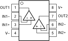
Pin Configurations: TLV1832-Q1 and TLV1842-Q1
 DGK, PW Packages
8-Pin VSSOP, TSSOP
Top View

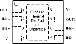
NOTE:
Connect exposed thermal pad directly to V-
pin.
DSG Package 8-Pad WSON With Exposed Thermal Pad,
Top View
Table 4-2 Pin Functions:
TLV1832-Q1
and TLV1842-Q1
| PIN | I/O | DESCRIPTION | |
|---|---|---|---|
| NAME |
NO. |
||
| OUT1 | 1 | O | Output pin of the comparator 1 |
| IN1– | 2 | I | Inverting input pin of comparator 1 |
| IN1+ | 3 | I | Noninverting input pin of comparator 1 |
| V- | 4 | — | Negative supply voltage |
| IN2+ | 5 | I | Noninverting input pin of comparator 2 |
| IN2– | 6 | I | Inverting input pin of comparator 2 |
| OUT2 | 7 | O | Output pin of the comparator 2 |
| V+ | 8 | — | Positive supply voltage |