SNOSDG6 September   2024 TLV1831-Q1

ADVANCE INFORMATION  

  1.   1
  2. Features
  3. Applications
  4. Description
  5. Pin Configuration and Functions
    1.     Pin Configuration: TLV1831-Q1 and TLV1841-Q1
    2.     Pin Configurations: TLV1832-Q1 and TLV1842-Q1
    3.     Pin Configuration and Functions: TLV1834-Q1 and TLV1844-Q1
  6. Specifications
    1. 5.1 Absolute Maximum Ratings
    2. 5.2 ESD Ratings
    3. 5.3 Thermal Information
    4. 5.4 Recommended Operating Conditions
    5. 5.5 Electrical Characteristics
    6. 5.6 Switching Characteristics
    7. 5.7 Typical Characteristics
  7. Detailed Description
    1. 6.1 Overview
    2. 6.2 Functional Block Diagrams
    3. 6.3 Feature Description
    4. 6.4 Device Functional Modes
      1. 6.4.1 Inputs
        1. 6.4.1.1 Rail-to-Rail Input
        2. 6.4.1.2 Unused Inputs
      2. 6.4.2 Outputs
        1. 6.4.2.1 TLV183x-Q1 Push-Pull Output
        2. 6.4.2.2 TLV184x-Q1 Open-Drain Output
      3. 6.4.3 ESD Protection
        1. 6.4.3.1 Inputs
        2. 6.4.3.2 Outputs
      4. 6.4.4 Power-On Reset (POR)
  8. Application and Implementation
    1. 7.1 Application Information
      1. 7.1.1 Basic Comparator Definitions
        1. 7.1.1.1 Operation
        2. 7.1.1.2 Propagation Delay
        3. 7.1.1.3 Overdrive Voltage
      2. 7.1.2 Hysteresis
        1. 7.1.2.1 Inverting Comparator With Hysteresis
        2. 7.1.2.2 Non-Inverting Comparator With Hysteresis
        3. 7.1.2.3 Inverting and Non-Inverting Hysteresis using Open-Drain Output
    2. 7.2 Typical Applications
      1. 7.2.1 Window Comparator
        1. 7.2.1.1 Design Requirements
        2. 7.2.1.2 Detailed Design Procedure
        3. 7.2.1.3 Application Curve
      2. 7.2.2 Square Wave Oscillator
        1. 7.2.2.1 Design Requirements
        2. 7.2.2.2 Detailed Design Procedure
        3. 7.2.2.3 Application Performance Plots
    3. 7.3 Power Supply Recommendations
    4. 7.4 Layout
      1. 7.4.1 Layout Guidelines
      2. 7.4.2 Layout Example
  9. Device and Documentation Support
    1. 8.1 Documentation Support
      1. 8.1.1 Related Documentation
    2. 8.2 Receiving Notification of Documentation Updates
    3. 8.3 Support Resources
    4. 8.4 Trademarks
    5. 8.5 Electrostatic Discharge Caution
    6. 8.6 Glossary
  10. Revision History
  11. 10Mechanical, Packaging, and Orderable Information

封装选项

机械数据 (封装 | 引脚)
散热焊盘机械数据 (封装 | 引脚)
订购信息

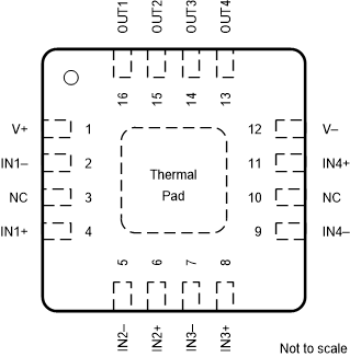
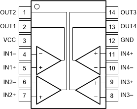
Pin Configuration and Functions: TLV1834-Q1 and TLV1844-Q1

TLV1831-Q1 TLV1841-Q1 TLV1832-Q1 TLV1842-Q1  DYY Package14-Pin SOT-23Top
                        ViewDYY Package
14-Pin SOT-23
Top View
TLV1831-Q1 TLV1841-Q1 TLV1832-Q1 TLV1842-Q1  RTE Package, 16-Pad WQFN With Exposed Thermal Pad
                            Top
                            View
NOTE: Connect exposed thermal pad directly to V- pin.
RTE Package,
16-Pad WQFN With Exposed Thermal Pad
Top View
Table 4-3 Pin Functions: TLV1834-Q1 and TLV1844-Q1
PINI/ODESCRIPTION
NAMESOT-23WQFN
OUT2115

O

Output pin of the comparator 2
OUT1216OOutput pin of the comparator 1
V+31

-

Positive supply voltage
IN1-42IInverting input pin of the comparator 1
IN1+54INoninverting input pin of the comparator 1
IN2-65IInverting input pin of the comparator 2
IN2+76INoninverting input pin of the comparator 2
IN3-87IInverting input pin of the comparator 3
IN3+98INoninverting input pin of the comparator 3
IN4-109IInverting input pin of the comparator 4
IN4+1111INoninverting input pin of the comparator 4
V-1212-Negative supply voltage
OUT41313OOutput pin of the comparator 4
OUT31414OOutput pin of the comparator 3
NC-3-No internal connection - leave floating or GND
NC-10-No internal connection - leave floating or GND
Thermal Pad-PAD-Connect directly to V- pin