ZHCSQ91 august   2023 TLV1851-Q1 , TLV1861-Q1

PRODMIX  

  1.   1
  2. 特性
  3. 应用
  4. 说明
  5. Revision History
  6. Pin Configuration and Functions
    1.     Pin Configuration: TLV1851-Q1 and TLV1861-Q1
    2.     Pin Configurations: TLV1852-Q1 and TLV1862-Q1
    3.     Pin Configurations: TLV1854-Q1 and TLV1864-Q1
  7. Specifications
    1. 6.1 Absolute Maximum Ratings
    2. 6.2 ESD Ratings
    3. 6.3 Thermal Information
    4. 6.4 Recommended Operating Conditions
    5. 6.5 Electrical Characteristics
    6. 6.6 Switching Characteristics
    7. 6.7 Typical Characteristics
  8. Detailed Description
    1. 7.1 Overview
    2. 7.2 Functional Block Diagrams
    3. 7.3 Feature Description
    4. 7.4 Device Functional Modes
      1. 7.4.1 Inputs
        1. 7.4.1.1 Operating Common-Mode Ranges
        2. 7.4.1.2 Fail-Safe Inputs
        3. 7.4.1.3 Unused Inputs
      2. 7.4.2 Internal Hysteresis
      3. 7.4.3 Outputs
        1. 7.4.3.1 TLV185x-Q1 Push-Pull Output
        2. 7.4.3.2 TLV186x-Q1 Open-Drain Output
      4. 7.4.4 ESD Protection
        1. 7.4.4.1 Inputs
        2. 7.4.4.2 Outputs
      5. 7.4.5 Power-On Reset (POR)
      6. 7.4.6 Reverse Battery Protection
  9. Application and Implementation
    1. 8.1 Application Information
      1. 8.1.1 Basic Comparator Definitions
        1. 8.1.1.1 Operation
        2. 8.1.1.2 Propagation Delay
        3. 8.1.1.3 Overdrive Voltage
      2. 8.1.2 Hysteresis
        1. 8.1.2.1 Inverting Comparator With Hysteresis
        2. 8.1.2.2 Non-Inverting Comparator With Hysteresis
        3. 8.1.2.3 Inverting and Non-Inverting Hysteresis using Open-Drain Output
    2. 8.2 Typical Applications
      1. 8.2.1 Window Comparator
        1. 8.2.1.1 Design Requirements
        2. 8.2.1.2 Detailed Design Procedure
        3. 8.2.1.3 Application Curve
      2. 8.2.2 Undervoltage Detection
      3. 8.2.3 Reverse Battery and Overvoltage Protection Scheme
    3. 8.3 Power Supply Recommendations
  10. Layout
    1. 9.1 Layout Guidelines
    2. 9.2 Layout Example
  11. 10器件和文档支持
    1. 10.1 Documentation Support
      1. 10.1.1 Related Documentation
    2. 10.2 接收文档更新通知
    3. 10.3 支持资源
    4. 10.4 Trademarks
    5. 10.5 静电放电警告
    6. 10.6 术语表
  12. 11Mechanical, Packaging, and Orderable Information

封装选项

机械数据 (封装 | 引脚)
散热焊盘机械数据 (封装 | 引脚)
订购信息

Internal Hysteresis

The device hysteresis transfer curve is shown in Figure 8-5. This curve is a function of three components: VTH, VOS, and VHYST:

  • VTH is the actual set voltage or threshold trip voltage.
  • VOS is the internal offset voltage between VIN+ and VIN–. This voltage is added to VTH to form the actual trip point at which the comparator must respond to change output states.
  • VHYST is the internal hysteresis (or trip window) that is designed to reduce comparator sensitivity to noise.

    (2.8 mV for the TLV185x/6x family)
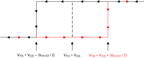
GUID-33C84EC9-3C5A-47AA-8FF2-8F1645DCDE77-low.gifFigure 7-2 Hysteresis Transfer Curve