SBOS935B April 2020 – July 2020 TLV197-Q1 , TLV2197-Q1 , TLV4197-Q1
PRODUCTION DATA.
- 1 Features
- 2 Applications
- 3 Description
- 4 Revision History
- 5 Pin Configuration and Functions
-
6 Specifications
- 6.1 Absolute Maximum Ratings
- 6.2 ESD Ratings
- 6.3 Recommended Operating Conditions
- 6.4 Thermal Information: TLV197-Q1
- 6.5 Thermal Information: TLV2197-Q1
- 6.6 Thermal Information: TLV4197-Q1
- 6.7 Electrical Characteristics: VS = ±4 V to ±18 V (VS = 8 V to 36 V)
- 6.8 Electrical Characteristics: VS = ±2.25 V to ±4 V (VS = 4.5 V to 8 V)
- 6.9 Typical Characteristics
- 7 Detailed Description
- 8 Application and Implementation
- 9 Power Supply Recommendations
- 10Layout
- 11Device and Documentation Support
- 12Mechanical, Packaging, and Orderable Information
8.2.1 16-Bit Precision Multiplexed Data-Acquisition System
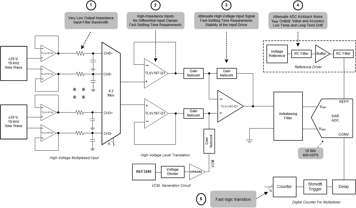
Figure 41 shows a 16-bit, differential, 4-channel, multiplexed data-acquisition system. This example is typical in sensor based applications that require low distortion and a high-voltage differential input. The circuit uses the ADS8864, a 16-bit, 400-kSPS successive-approximation-resistor (SAR) analog-to-digital converter (ADC), along with a precision, high-voltage, signal-conditioning front end, and a 4-channel differential multiplexer (mux). This TI Precision Design details the process for optimizing the precision, high-voltage, front-end drive circuit using the TLVx197-Q1 and TLV140 to achieve excellent dynamic performance and linearity with the ADS8864.
 Figure 41. TLVx197-Q1 in 16-Bit, 400-kSPS, 4-Channel, Multiplexed Data Acquisition System for High-Voltage Inputs With Lowest Distortion