SBOS935B April 2020 – July 2020 TLV197-Q1 , TLV2197-Q1 , TLV4197-Q1
PRODUCTION DATA.
- 1 Features
- 2 Applications
- 3 Description
- 4 Revision History
- 5 Pin Configuration and Functions
-
6 Specifications
- 6.1 Absolute Maximum Ratings
- 6.2 ESD Ratings
- 6.3 Recommended Operating Conditions
- 6.4 Thermal Information: TLV197-Q1
- 6.5 Thermal Information: TLV2197-Q1
- 6.6 Thermal Information: TLV4197-Q1
- 6.7 Electrical Characteristics: VS = ±4 V to ±18 V (VS = 8 V to 36 V)
- 6.8 Electrical Characteristics: VS = ±2.25 V to ±4 V (VS = 4.5 V to 8 V)
- 6.9 Typical Characteristics
- 7 Detailed Description
- 8 Application and Implementation
- 9 Power Supply Recommendations
- 10Layout
- 11Device and Documentation Support
- 12Mechanical, Packaging, and Orderable Information
7.3.4 Thermal Protection
CAUTION
The absolute maximum junction temperature of the TLVx197-Q1 is 150°C. Exceeding this temperature causes damage to the device.
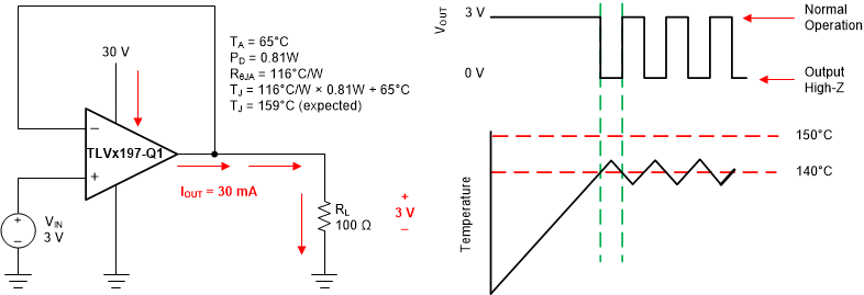
The internal power dissipation of any amplifier causes the internal (junction) temperature of the amplifier to rise. This phenomenon is called self heating. The TLVx197-Q1 has a thermal protection feature that prevents damage from self heating. The protection works by monitoring the temperature of the device and turning off the op amp output drive for temperatures greater than 140°C. Figure 37 shows an application example for the TLVx197-Q1 that has significant self heating (159°C) because of the power dissipation (0.81 W). Thermal calculations indicate that for an ambient temperature of 65°C, the device junction temperature must reach 187°C. The actual device, however, turns off the output drive to maintain a safe junction temperature. Figure 37 shows how the circuit behaves during thermal protection. During normal operation, the device acts as a buffer, so the output is 3 V. When self heating causes the device junction temperature to exceed 140°C, the thermal protection forces the output to a high-impedance state, and the output is pulled to ground through resistor RL.
 Figure 37. Thermal Protection