SBOS935B April   2020  – July 2020 TLV197-Q1 , TLV2197-Q1 , TLV4197-Q1

PRODUCTION DATA.  

  1. Features
  2. Applications
  3. Description
    1.     Device Images
      1.      TLVx197-Q1 Detect Voltages in Automotive Applications
  4. Revision History
  5. Pin Configuration and Functions
    1.     Pin Functions: TLV197-Q1
    2.     Pin Functions: TLV2197-Q1
    3.     Pin Functions: TLV4197-Q1
  6. Specifications
    1. 6.1 Absolute Maximum Ratings
    2. 6.2 ESD Ratings
    3. 6.3 Recommended Operating Conditions
    4. 6.4 Thermal Information: TLV197-Q1
    5. 6.5 Thermal Information: TLV2197-Q1
    6. 6.6 Thermal Information: TLV4197-Q1
    7. 6.7 Electrical Characteristics: VS = ±4 V to ±18 V (VS = 8 V to 36 V)
    8. 6.8 Electrical Characteristics: VS = ±2.25 V to ±4 V (VS = 4.5 V to 8 V)
    9. 6.9 Typical Characteristics
  7. Detailed Description
    1. 7.1 Overview
    2. 7.2 Functional Block Diagram
    3. 7.3 Feature Description
      1. 7.3.1 Input Protection Circuitry
      2. 7.3.2 EMI Rejection
      3. 7.3.3 Phase Reversal Protection
      4. 7.3.4 Thermal Protection
      5. 7.3.5 Capacitive Load and Stability
      6. 7.3.6 Common-Mode Voltage Range
      7. 7.3.7 Electrical Overstress
      8. 7.3.8 Overload Recovery
    4. 7.4 Device Functional Modes
  8. Application and Implementation
    1. 8.1 Application Information
    2. 8.2 Typical Applications
      1. 8.2.1 16-Bit Precision Multiplexed Data-Acquisition System
        1. 8.2.1.1 Design Requirements
        2. 8.2.1.2 Detailed Design Procedure
        3. 8.2.1.3 Application Curve
      2. 8.2.2 Slew-Rate Limit for Input Protection
      3. 8.2.3 Precision Reference Buffer
  9. Power Supply Recommendations
  10. 10Layout
    1. 10.1 Layout Guidelines
    2. 10.2 Layout Examples
  11. 11Device and Documentation Support
    1. 11.1 Device Support
      1. 11.1.1 Development Support
        1. 11.1.1.1 TINA-TI (Free Software Download)
    2. 11.2 Documentation Support
      1. 11.2.1 Related Documentation
    3. 11.3 Related Links
    4. 11.4 Receiving Notification of Documentation Updates
    5. 11.5 Support Resources
    6. 11.6 Trademarks
    7. 11.7 Electrostatic Discharge Caution
    8. 11.8 Glossary
  12. 12Mechanical, Packaging, and Orderable Information

封装选项

机械数据 (封装 | 引脚)
散热焊盘机械数据 (封装 | 引脚)
订购信息

Typical Characteristics

at TA = 25°C, VS = ±18 V, VCM = VS / 2, RLOAD = 10 kΩ connected to VS / 2, and CL = 100 pF (unless otherwise noted)
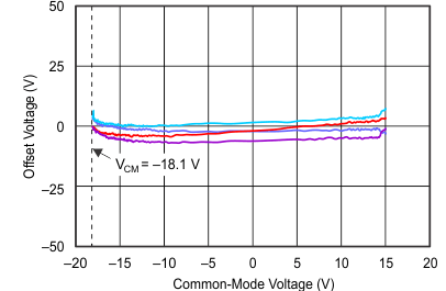
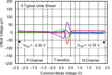
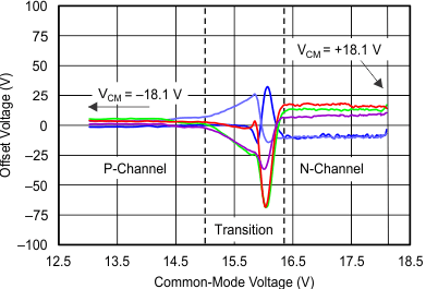
TLV197-Q1 TLV2197-Q1 TLV4197-Q1 C002_OT.gif
Figure 1. Offset Voltage vs Common-Mode Voltage
TLV197-Q1 TLV2197-Q1 TLV4197-Q1 sbos850_c005_ot.gif
VS = ±2.25 V
Figure 3. Offset Voltage vs Common-Mode Voltage
TLV197-Q1 TLV2197-Q1 TLV4197-Q1 sbos850_c004_sbos620.gif
CLOAD = 15 pF
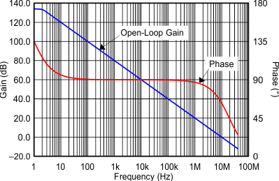
Figure 5. Open-Loop Gain and Phase vs Frequency
TLV197-Q1 TLV2197-Q1 TLV4197-Q1 C017_OT.gif
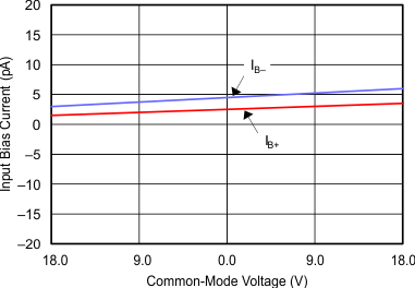
Figure 7. Input Bias Current vs Common-Mode Voltage
TLV197-Q1 TLV2197-Q1 TLV4197-Q1 C018_OT.gif
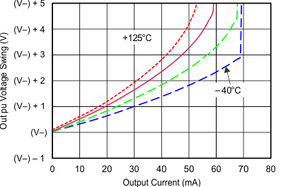
Figure 9. Output Voltage Swing vs Output Current (Maximum Supply)
TLV197-Q1 TLV2197-Q1 TLV4197-Q1 C008_OT.png
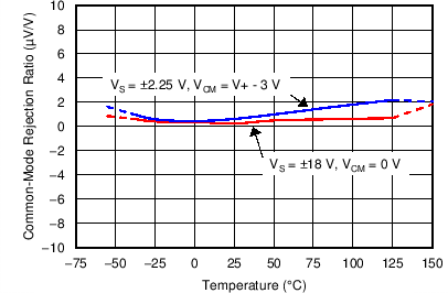
Figure 11. CMRR vs Temperature
TLV197-Q1 TLV2197-Q1 TLV4197-Q1 C001_SBOS620.gif
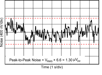
Figure 13. 0.1-Hz to 10-Hz Noise
TLV197-Q1 TLV2197-Q1 TLV4197-Q1 sbos850_c007_sbos620.gif
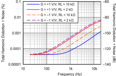
VOUT = 3.5 VRMS, BW = 80 kHz
Figure 15. THD+N Ratio vs Frequency
TLV197-Q1 TLV2197-Q1 TLV4197-Q1 C012_OT.gif
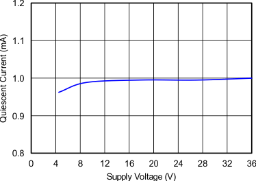
Figure 17. Quiescent Current vs Supply Voltage
TLV197-Q1 TLV2197-Q1 TLV4197-Q1 sbos850_c009_ot.gif
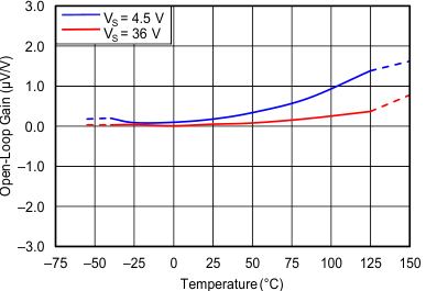
RL = 10 kΩ
Figure 19. Open-Loop Gain vs Temperature
TLV197-Q1 TLV2197-Q1 TLV4197-Q1 c013_sbos935.gif
RI = 1 kΩ, RF = 1 kΩ, G = –1
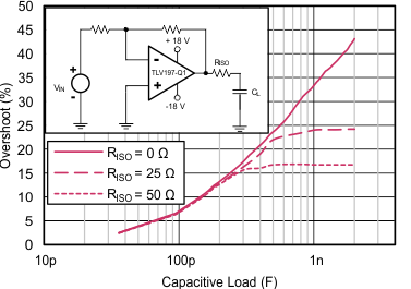
Figure 21. Small-Signal Overshoot vs Capacitive Load
(100-mV Output Step)
TLV197-Q1 TLV2197-Q1 TLV4197-Q1 c009_sbos935.gif
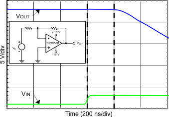
RI = 1 kΩ, RF = 10 kΩ, G = –10
Figure 23. Positive Overload Recovery
TLV197-Q1 TLV2197-Q1 TLV4197-Q1 c006_sbos935.gif
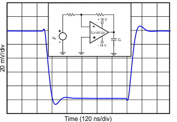
RL = 1 kΩ, CL = 10 pF, G = –1
Figure 25. Small-Signal Step Response (100 mV)
TLV197-Q1 TLV2197-Q1 TLV4197-Q1 sbos850_c034_.gif
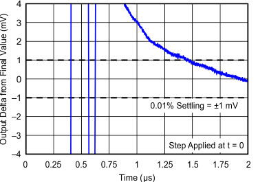
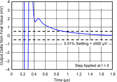
G = 1
Figure 27. Settling Time (10-V Positive Step)
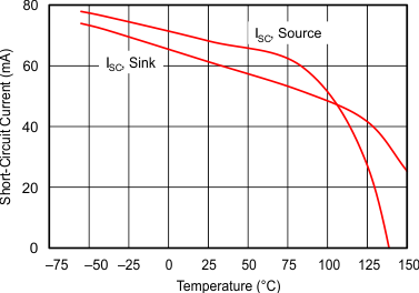
TLV197-Q1 TLV2197-Q1 TLV4197-Q1 C016_OT.gif
Figure 29. Short-Circuit Current vs Temperature
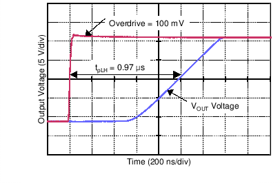
TLV197-Q1 TLV2197-Q1 TLV4197-Q1 C025_.png
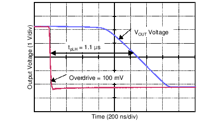
Figure 31. Propagation Delay Rising Edge
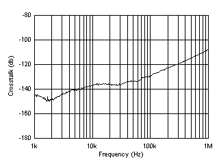
TLV197-Q1 TLV2197-Q1 TLV4197-Q1 D001_SBOS620.gif
Figure 33. Crosstalk vs Frequency
TLV197-Q1 TLV2197-Q1 TLV4197-Q1 C003_OT.gif
Figure 2. Offset Voltage vs Common-Mode Voltage
TLV197-Q1 TLV2197-Q1 TLV4197-Q1 sbos850_c006_ot.gif
VS = ±2.25 V to ±18 V
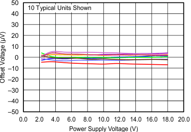
Figure 4. Offset Voltage vs Power Supply
TLV197-Q1 TLV2197-Q1 TLV4197-Q1 C003_SBOS620.png
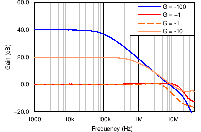
Figure 6. Closed-Loop Gain and Phase vs Frequency
TLV197-Q1 TLV2197-Q1 TLV4197-Q1 C015_OT.png
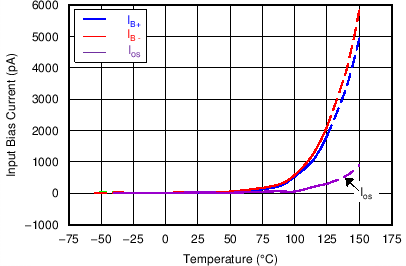
Figure 8. Input Bias Current vs Temperature
TLV197-Q1 TLV2197-Q1 TLV4197-Q1 C012_SBOS620.png
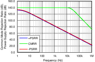
Figure 10. CMRR and PSRR vs Frequency
TLV197-Q1 TLV2197-Q1 TLV4197-Q1 C007_OT.gif
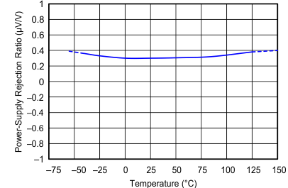
Figure 12. PSRR vs Temperature
TLV197-Q1 TLV2197-Q1 TLV4197-Q1 C002_SBOS620.gif
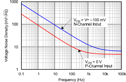
Figure 14. Input Voltage Noise Spectral Density
vs Frequency
TLV197-Q1 TLV2197-Q1 TLV4197-Q1 sbos850_c008_sbos620.gif
f = 1 kHz, BW = 80 kHz
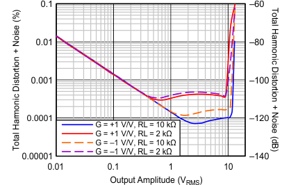
Figure 16. THD+N vs Output Amplitude
TLV197-Q1 TLV2197-Q1 TLV4197-Q1 C011_OT.gif
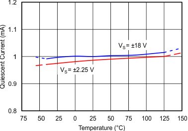
Figure 18. Quiescent Current vs Temperature
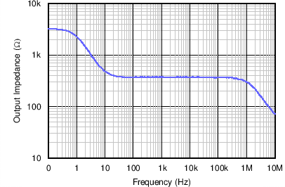
TLV197-Q1 TLV2197-Q1 TLV4197-Q1 C016_SBOS620.png
Figure 20. Open-Loop Output Impedance vs Frequency
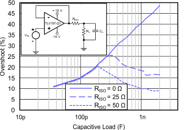
TLV197-Q1 TLV2197-Q1 TLV4197-Q1 c013b_sbos935.gif
G = 1
Figure 22. Small-Signal Overshoot vs Capacitive Load
(100-mV Output Step)
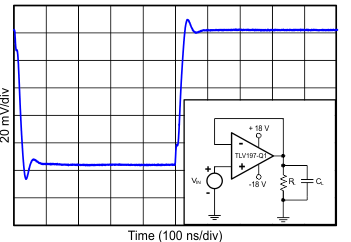
TLV197-Q1 TLV2197-Q1 TLV4197-Q1 c015_sbos935.gif
CL = 10 pF, G = 1
Figure 24. Small-Signal Step Response (100 mV)
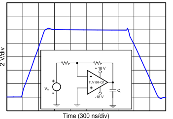
TLV197-Q1 TLV2197-Q1 TLV4197-Q1 c005_sbos935.gif
RL = 1 kΩ, CL = 10 pF, G = –1
Figure 26. Large-Signal Step Response
TLV197-Q1 TLV2197-Q1 TLV4197-Q1 sbos850_c034b_.gif
G = 1
Figure 28. Settling Time (5-V Positive Step)
TLV197-Q1 TLV2197-Q1 TLV4197-Q1 C033_.png
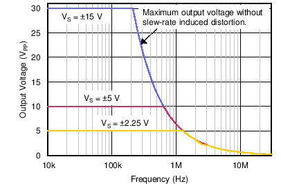
Figure 30. Maximum Output Voltage vs Frequency
TLV197-Q1 TLV2197-Q1 TLV4197-Q1 C026_.png
Figure 32. Propagation Delay Falling Edge