ZHCSK18 July   2019 TLV2186

PRODUCTION DATA.  

  1. 特性
  2. 应用
  3. 说明
    1.     Device Images
      1.      高侧电流分流监控器应用
      2.      VOS 与输入共模电压
  4. 修订历史记录
  5. Pin Configuration and Functions
    1.     Pin Functions
  6. Specifications
    1. 6.1 Absolute Maximum Ratings
    2. 6.2 ESD Ratings
    3. 6.3 Recommended Operating Conditions
    4. 6.4 Thermal Information
    5. 6.5 Electrical Characteristics
    6. 6.6 Typical Characteristics
  7. Detailed Description
    1. 7.1 Overview
    2. 7.2 Functional Block Diagram
    3. 7.3 Feature Description
      1. 7.3.1 Rail-to-Rail Inputs
      2. 7.3.2 Phase-Reversal Protection
      3. 7.3.3 Input Bias Current Clock Feedthrough
      4. 7.3.4 EMI Rejection
        1. 7.3.4.1 EMIRR +IN Test Configuration
      5. 7.3.5 Electrical Overstress
      6. 7.3.6 MUX-Friendly Inputs
    4. 7.4 Device Functional Modes
  8. Application and Implementation
    1. 8.1 Application Information
      1. 8.1.1 Basic Noise Calculations
    2. 8.2 Typical Applications
      1. 8.2.1 High-Side Current Sensing
        1. 8.2.1.1 Design Requirements
        2. 8.2.1.2 Detailed Design Procedure
        3. 8.2.1.3 Application Curve
      2. 8.2.2 Bridge Amplifier
      3. 8.2.3 Low-Side Current Monitor
      4. 8.2.4 RTD Amplifier With Linearization
  9. Power Supply Recommendations
  10. 10Layout
    1. 10.1 Layout Guidelines
    2. 10.2 Layout Example
  11. 11器件和文档支持
    1. 11.1 器件支持
      1. 11.1.1 开发支持
        1. 11.1.1.1 TINA-TI(免费软件下载)
        2. 11.1.1.2 TI 高精度设计
    2. 11.2 文档支持
      1. 11.2.1 相关文档
    3. 11.3 接收文档更新通知
    4. 11.4 社区资源
    5. 11.5 商标
    6. 11.6 静电放电警告
    7. 11.7 Glossary
  12. 12机械、封装和可订购信息

封装选项

机械数据 (封装 | 引脚)
散热焊盘机械数据 (封装 | 引脚)
订购信息

Typical Characteristics

Table 1. Typical Characteristic Graphs

DESCRIPTION FIGURE
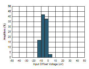
Offset Voltage Distribution Figure 1
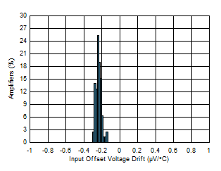
Offset Voltage Drift (-40°C to +125C°C) Figure 2
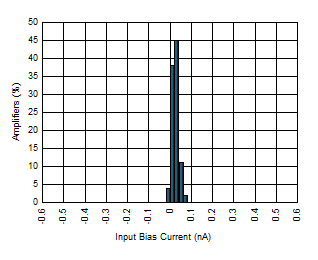
Input Bias Current Distribution Figure 3
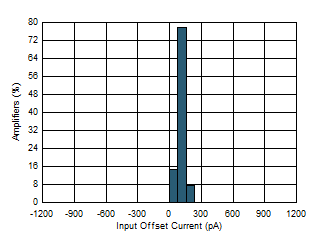
Input Offset Current Distribution Figure 4
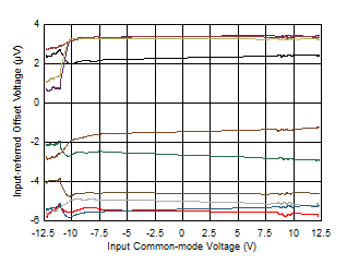
Offset Voltage vs Common-Mode Voltage Figure 5
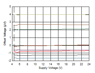
Offset Voltage vs Supply Voltage Figure 6
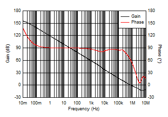
Open-Loop Gain and Phase vs Frequency Figure 7
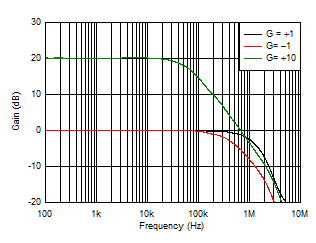
Closed-Loop Gain vs Frequency Figure 8
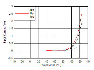
Input Bias Current and Offset Current vs Temperature Figure 9
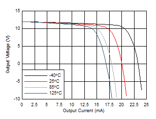
Output Voltage Swing vs Output Current (Sourcing) Figure 10
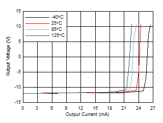
Output Voltage Swing vs Output Current (Sinking) Figure 11
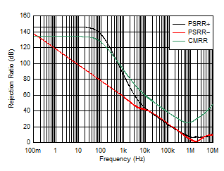
CMRR and PSRR vs Frequency Figure 12
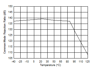
CMRR vs Temperature Figure 13
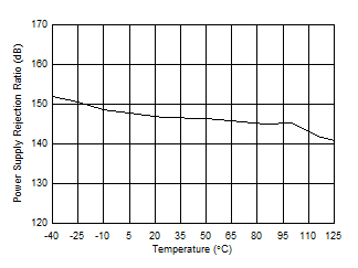
PSRR vs Temperature Figure 14
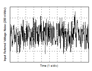
0.1-Hz to 10-Hz Voltage Noise Figure 15
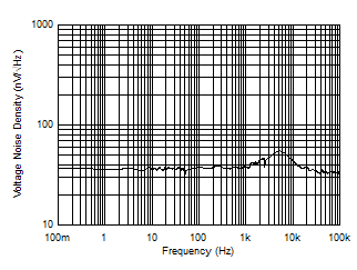
Input Voltage Noise Spectral Density vs Frequency Figure 16
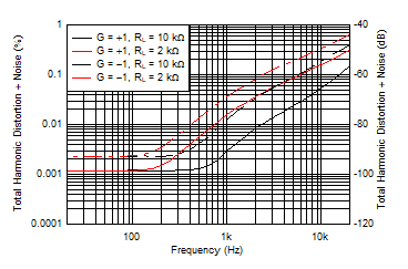
THD+N vs Frequency Figure 17
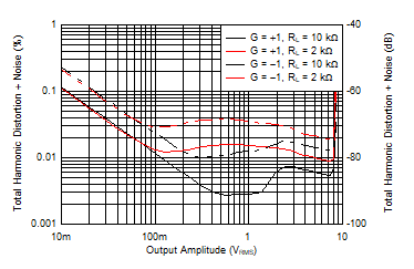
THD+N vs Output Amplitude Figure 18
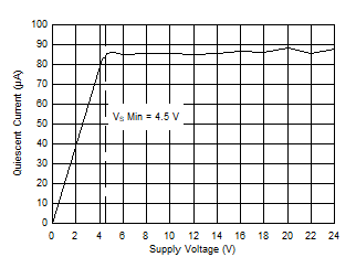
Quiescent Current vs Supply Voltage Figure 19
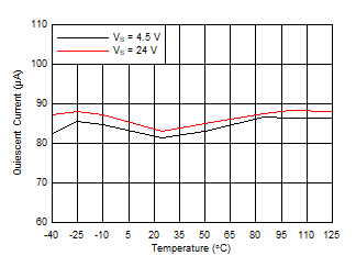
Quiescent Current vs Temperature Figure 20
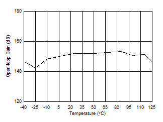
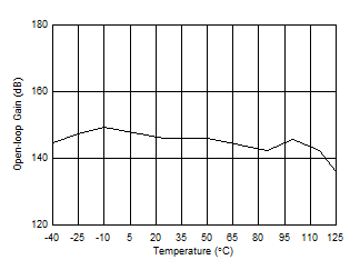
Open-Loop Gain vs Temperature (10 kΩ) Figure 21
Open-Loop Gain vs Temperature (2 kΩ) Figure 22
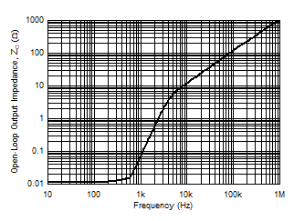
Open-Loop Output Impedance vs Frequency Figure 23
Small-Signal Overshoot vs Capacitive Load (Gain = –1, 10-mV step) Figure 24
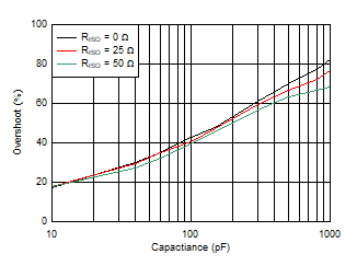
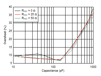
Small-Signal Overshoot vs Capacitive Load (Gain = 1, 10-mV step) Figure 25
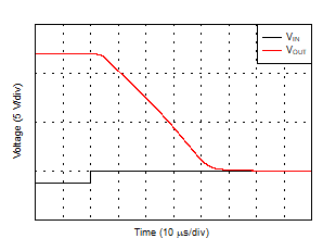
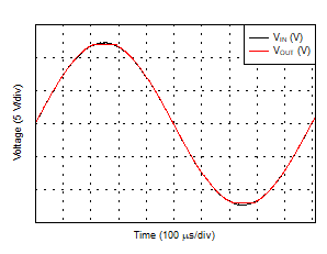
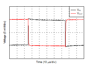
No Phase Reversal Figure 26
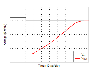
Positive Overload Recovery Figure 27
Negative Overload Recovery Figure 28
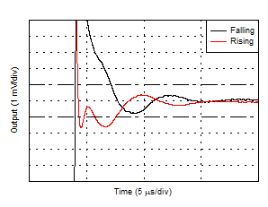
Small-Signal Step Response (Gain = 1, 10-mV step) Figure 29
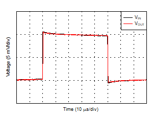
Small-Signal Step Response (Gain = –1, 10-mV step) Figure 30
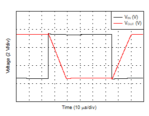
Large-Signal Step Response (Gain = 1, 10-V step) Figure 31
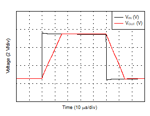
Large-Signal Step Response (Gain = –1, 10-V step) Figure 32
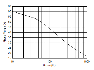
Phase Margin vs Capacitive Load Figure 33
Settling Time (1-V Step, 0.1% Settling) Figure 34
Short Circuit Current vs Temperature Figure 35
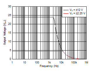
Maximum Output Voltage vs Frequency Figure 36
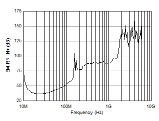
EMIRR vs Frequency Figure 37
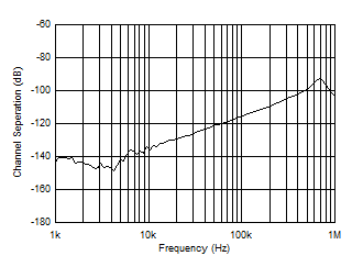
Channel Separation Figure 38
at TA = 25°C, VS = ±12 V, VCM = VS / 2, RL = 10 kΩ (unless otherwise noted)
TLV2186 D001_VOS.gif
Figure 1. Offset Voltage Distribution
TLV2186 Histogram_Ib_25C.gif
Figure 3. Input Bias Current Distribution
TLV2186 D017_Linear_VosvsVcm_25C.gif
Figure 5. Offset Voltage vs Common-Mode Voltage
TLV2186 D004_Aol_Gain_Phase.gif
Figure 7. Open-Loop Gain and Phase vs Frequency
TLV2186 D022_Linear_IB_IOSvsTemperature.gif
Figure 9. Input Bias Current and Offset Current vs Temperature
TLV2186 Sinking_Vout_vs_Iout.gif
Figure 11. Output Voltage Swing vs Output Current (Sinking)
TLV2186 D025_Linear_CMRRvsTemperature.gif
Figure 13. CMRR vs Temperature
TLV2186 D027_p1_10Hz_Noise.gif
Figure 15. 0.1-Hz to 10-Hz Voltage Noise
TLV2186 D009_THDN_Freq.gif
Figure 17. THD+N vs Frequency
TLV2186 D028_Linear_IQvsSupply.gif
Figure 19. Quiescent Current vs Supply Voltage
TLV2186 D030B_Linear_AOL_10KvsTemp.gif
Figure 21. Open-Loop Gain vs Temperature
TLV2186 D011_OpenLoopOutputImp.gif
Figure 23. Open-Loop Output Impedance vs Frequency
TLV2186 D032_NonInverting_Overshoot.gif
Gain = 1, 10-mV step
Figure 25. Small-Signal Overshoot vs Capacitive Load
TLV2186 D034B_Positive_Overload.gif
Figure 27. Positive Overload Recovery
TLV2186 D035A_SmallSignal_10mV_G1.gif
Gain = 1, 10-mV step
Figure 29. Small-Signal Step Response
TLV2186 D036A_LargeSignal_5V_G1.gif
Gain = 1, 10-V step
Figure 31. Large-Signal Step Response
TLV2186 D005_PhaseMargin_Cload.gif
Figure 33. Phase Margin vs Capacitive Load
TLV2186 Linear_ISC_vs_Temperature.gif
Figure 35. Short Circuit Current vs Temperature
TLV2186 D014_EMIRR.gif
Figure 37. EMIRR vs Frequency
TLV2186 D003_HistogramVOS_Drift.gif
Figure 2. Offset Voltage Drift (-40°C to 125C°C)
TLV2186 D040_IOS.gif
Figure 4. Input Offset Current Distribution
TLV2186 D020_Linear_VosvsVs_25C.gif
Figure 6. Offset Voltage vs Supply Voltage
TLV2186 D006_ClosedLoopGain.gif
Figure 8. Closed-Loop Gain vs Frequency
TLV2186 Sourcing_Vout_vs_Iout.gif
Figure 10. Output Voltage Swing vs Output Current (Sourcing)
TLV2186 D007_PSRR_CMRR.gif
Figure 12. CMRR and PSRR vs Frequency
TLV2186 D026_Linear_PSRRvsTemperature.gif
Figure 14. PSRR vs Temperature
TLV2186 D008_VoltageNoise.gif
Figure 16. Input Voltage Noise Spectral Density vs Frequency
TLV2186 D010_THDN_Vrms.gif
Figure 18. THD+N vs Output Amplitude
TLV2186 D029_Linear_IQvsTemperature.gif
Figure 20. Quiescent Current vs Temperature
TLV2186 D030A_Linear_AOL_2KvsTemp.gif
RL = 2 kΩ
Figure 22. Open-Loop Gain vs Temperature
TLV2186 D031_Inverting_Overshoot.gif
Gain = –1, 10-mV step
Figure 24. Small-Signal Overshoot vs Capacitive Load
TLV2186 D033_NoPhaseReversal.gif
Figure 26. No Phase Reversal
TLV2186 D034A_Negative_Overload.gif
Figure 28. Negative Overload Recovery
TLV2186 D035B_SmallSignal_10mV_G-1.gif
Gain = –1, 10-mV step
Figure 30. Small-Signal Step Response
TLV2186 D036B_LargeSignal_5V_G-1.gif
Gain = –1, 10-V step
Figure 32. Large-Signal Step Response
TLV2186 D037_SettlingTime_1V_p1Percent.gif
1-V step, 0.1% settling
Figure 34. Settling Time
TLV2186 D012_FulPowerBandwidth.gif
Figure 36. Maximum Output Voltage vs Frequency
TLV2186 D013_ChannelSeparation.gif
Figure 38. Channel Separation