SLVS067M March 1992 – November 2016 TLV2217
PRODUCTION DATA.
- 1 Features
- 2 Applications
- 3 Description
- 4 Revision History
- 5 Pin Configuration and Functions
- 6 Specifications
- 7 Detailed Description
- 8 Application and Implementation
- 9 Power Supply Recommendations
- 10Layout
- 11Device and Documentation Support
- 12Mechanical, Packaging, and Orderable Information
封装选项
请参考 PDF 数据表获取器件具体的封装图。
机械数据 (封装 | 引脚)
- KVU|3
- KCS|3
- PW|20
散热焊盘机械数据 (封装 | 引脚)
- KVU|3
订购信息
8 Application and Implementation
NOTE
Information in the following applications sections is not part of the TI component specification, and TI does not warrant its accuracy or completeness. TI’s customers are responsible for determining suitability of components for their purposes. Customers should validate and test their design implementation to confirm system functionality.
8.1 Application Information
The TLV2217 is a low-dropout linear regulator and can be used as a fixed output voltage supply for a wide variety of applications up to 500 mA. The TLV2217 has multiple output voltage options including 1.8 V, 2.5 V, and 3.3 V. The TLV2217 requires a minimum of 3 V or (VO(max) + 0.5 V) input to ensure regulation and is characterized for operation over the virtual junction temperature range of 0°C to 125°C.
8.2 Typical Application
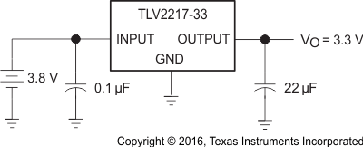
 Figure 2. Typical Application Schematic
8.2.1 Design Requirements
The input voltage must be high enough so that there is enough headroom for the output to regulate. This specification is defined as the dropout voltage in the Electrical Characteristics: TLV2217-33.
A 0.1-µF capacitor must be place on the input to stabilize the input supply, especially if the TLV2217 is not placed near the source of supply.
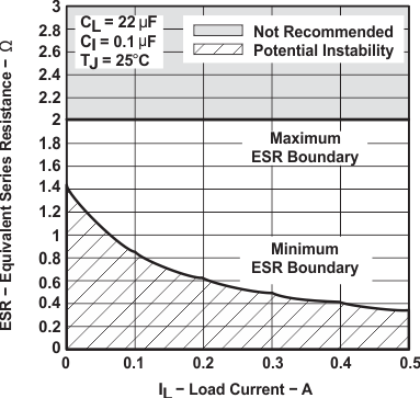
Output capacitor selection is critical for regulator stability. Larger COUT values benefit the regulator by improving transient response and loop stability. This device is designed to be stable with tantalum and aluminum electrolytic output capacitors having an ESR between 0.4 Ω and 2 Ω. See Compensation-Capacitor Selection Information for additional details regarding capacitor selection.
8.2.2 Detailed Design Procedure
8.2.2.1 Compensation-Capacitor Selection Information
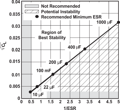
The TLV2217 is a low-dropout regulator. This means that the capacitance loading is important to the performance of the regulator because it is a vital part of the control loop. The capacitor value and the equivalent series resistance (ESR) both affect the control loop and must be defined for the load range and the temperature range. Figure 3 and Figure 4 can be used to establish the capacitance value and ESR range for the best regulator performance.
 Figure 3. TLV2217 ESR of Output Capacitor
vs Load Current
 Figure 4. TLV2217 Stability vs ESR
8.2.2.2 High Start-up Current
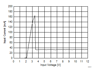
Due to the structure of the TLV2217, a high peak current is required on start-up. See Figure 5 for the input current characteristic.
NOTE
When the TLV2217 is starting up, it has to overcome the peak current to start regulating at the output. Due to the peak current required for the TLV2217, a resistor connected in series with the input is not recommended, as the I*R drop across the resistor may cause the input voltage to drop below the required headroom for the device.
8.2.3 Application Curves
 Figure 5. Input Current vs Input Voltage