SLVS067M March   1992  – November 2016 TLV2217

PRODUCTION DATA.  

  1. Features
  2. Applications
  3. Description
  4. Revision History
  5. Pin Configuration and Functions
  6. Specifications
    1. 6.1 Absolute Maximum Ratings
    2. 6.2 ESD Ratings
    3. 6.3 Recommended Operating Conditions
    4. 6.4 Thermal Information
    5. 6.5 Electrical Characteristics: TLV2217-33
    6. 6.6 Electrical Characteristics: TLV2217-25
    7. 6.7 Electrical Characteristics: TLV2217-18
    8. 6.8 Typical Characteristics
  7. Detailed Description
    1. 7.1 Overview
    2. 7.2 Functional Block Diagram
    3. 7.3 Feature Description
      1. 7.3.1 Overload Block
    4. 7.4 Device Functional Modes
      1. 7.4.1 Operation With Low Input Voltage
      2. 7.4.2 Operation at Light Loads
      3. 7.4.3 Operation in Self Protection
  8. Application and Implementation
    1. 8.1 Application Information
    2. 8.2 Typical Application
      1. 8.2.1 Design Requirements
      2. 8.2.2 Detailed Design Procedure
        1. 8.2.2.1 Compensation-Capacitor Selection Information
        2. 8.2.2.2 High Start-up Current
      3. 8.2.3 Application Curves
  9. Power Supply Recommendations
  10. 10Layout
    1. 10.1 Layout Guidelines
    2. 10.2 Layout Example
  11. 11Device and Documentation Support
    1. 11.1 Receiving Notification of Documentation Updates
    2. 11.2 Community Resources
    3. 11.3 Trademarks
    4. 11.4 Electrostatic Discharge Caution
    5. 11.5 Glossary
  12. 12Mechanical, Packaging, and Orderable Information

封装选项

请参考 PDF 数据表获取器件具体的封装图。

机械数据 (封装 | 引脚)
  • KVU|3
  • KCS|3
  • PW|20
散热焊盘机械数据 (封装 | 引脚)
订购信息

Layout

Layout Guidelines

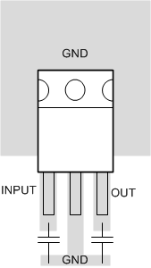
See Figure 6 for an example layout for the TLV2217 using the TO-220 package. Input and output bypass capacitors must be placed as close to the device pins as possible. The output capacitor must have a specified ESR in the range defined by Figure 4. Additionally, the ground pin and thermal tab must be well connected to a ground plane to aid in thermal dissipation.

Layout Example

TLV2217 T0220layout_3pin.gif Figure 6. TO-220 Package Example Layout