SLAS354C September 2001 – September 2015 TLV2553
PRODUCTION DATA.
- 1 Features
- 2 Applications
- 3 Description
- 4 Revision History
- 5 Pin Configuration and Functions
-
6 Specifications
- 6.1 Absolute Maximum Ratings
- 6.2 ESD Ratings
- 6.3 Recommended Operating Conditions
- 6.4 Thermal Information
- 6.5 Electrical Characteristics
- 6.6 External Reference Specifications
- 6.7 Operating Characteristics
- 6.8 Timing Requirements: VREF+ = 5 V
- 6.9 Timing Requirements: VREF+ = 2.5 V
- 6.10 Typical Characteristics
- 7 Parameter Measurement Information
-
8 Detailed Description
- 8.1 Overview
- 8.2 Functional Block Diagram
- 8.3 Feature Description
- 8.4
Device Functional Modes
- 8.4.1 Converter Operation
- 8.4.2 Data I/O Cycle
- 8.4.3 Sampling Cycle
- 8.4.4 Conversion Cycle
- 8.4.5 Power Up and Initialization
- 8.4.6 Data Input
- 8.4.7 Data Input—Address/Command Bits
- 8.4.8 Data Output Length
- 8.4.9 LSB Out First
- 8.4.10 Bipolar Output Format
- 8.4.11 EOC Output
- 8.4.12 Chip-Select Input (CS)
- 8.4.13 Power-Down Features
- 9 Application and Implementation
- 10Power Supply Recommendations
- 11Layout
- 12Device and Documentation Support
- 13Mechanical, Packaging, and Orderable Information
11 Layout
11.1 Layout Guidelines
- All decoupling capacitors must be located as close as possible to the loads they are supplying.
- TI recommends large copper fill areas or thick traces wherever possible to provide low inductance current paths between decoupling capacitors and their loads
- Ensure that there are no vias or discontinuities in the forward or return current paths that can cause the current loop area and therefore the loop inductance to increase.
- For high-frequency current paths routed across PCB layers, multiple vias can be placed close together (but not obstructing the current path) to lower inductance.
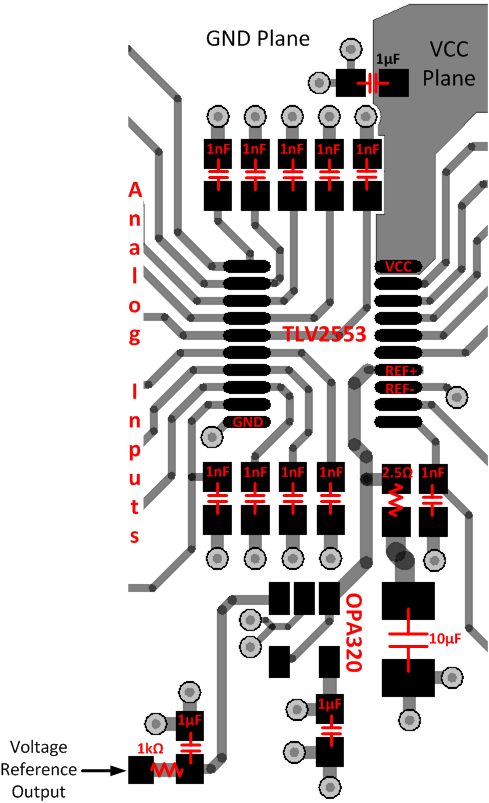
11.2 Layout Example
 Figure 43. Layout Example Schematic