ZHCSFZ5A February   2017  – December 2017 TLV3201-Q1 , TLV3202-Q1

PRODUCTION DATA.  

  1. 特性
  2. 应用
  3. 说明
    1.     Device Images
      1.      阈值检测器
      2.      传播延迟与过驱动
  4. 修订历史记录
  5. Device Comparison Table
  6. Pin Configuration and Functions
    1.     Pin Functions: TLV3201-Q1
    2.     Pin Functions: TLV3202-Q1
  7. Specifications
    1. 7.1 Absolute Maximum Ratings
    2. 7.2 ESD Ratings
    3. 7.3 Recommended Operating Conditions
    4. 7.4 Thermal Information
    5. 7.5 Electrical Characteristics: VCC = 5 V
    6. 7.6 Electrical Characteristics: VCC = 2.7 V
    7. 7.7 Switching Characteristics
    8. 7.8 Typical Characteristics
  8. Detailed Description
    1. 8.1 Overview
    2. 8.2 Functional Block Diagram
    3. 8.3 Feature Description
      1. 8.3.1 Operating Voltage
      2. 8.3.2 Input Overvoltage Protection
    4. 8.4 Device Functional Modes
  9. Application and Implementation
    1. 9.1 Application Information
      1. 9.1.1 Comparator Inputs
      2. 9.1.2 External Hysteresis
        1. 9.1.2.1 Inverting Comparator with Hysteresis
        2. 9.1.2.2 Noninverting Comparator With Hysteresis
      3. 9.1.3 Capacitive Loads
    2. 9.2 Typical Applications
      1. 9.2.1 TLV3201-Q1 Configured as an AC-Coupled Comparator
        1. 9.2.1.1 Design Requirements
        2. 9.2.1.2 Detailed Design Procedure
        3. 9.2.1.3 Application Curve
      2. 9.2.2 TLV3201-Q1 and OPA320 Configured as a Fast-Response Output Current Monitor
      3. 9.2.3 TLV3201-Q1 and TMP20 Configured as a Precision Analog Temperature Switch
  10. 10Power Supply Recommendations
  11. 11Layout
    1. 11.1 Layout Guidelines
    2. 11.2 Layout Example
  12. 12器件和文档支持
    1. 12.1 器件支持
      1. 12.1.1 开发支持
        1. 12.1.1.1 TINA-TI™ 仿真软件(免费下载)
        2. 12.1.1.2 通用运算放大器评估模块 (EVM)
        3. 12.1.1.3 TI 高精度设计
        4. 12.1.1.4 WEBENCH滤波器设计器
    2. 12.2 文档支持
      1. 12.2.1 相关文档
    3. 12.3 相关链接
    4. 12.4 接收文档更新通知
    5. 12.5 社区资源
    6. 12.6 商标
    7. 12.7 静电放电警告
    8. 12.8 Glossary
  13. 13机械、封装和可订购信息

封装选项

机械数据 (封装 | 引脚)
散热焊盘机械数据 (封装 | 引脚)
订购信息

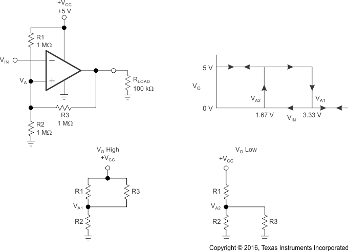
Inverting Comparator with Hysteresis

The inverting comparator with hysteresis requires a three-resistor network that is referenced to the comparator supply voltage (VCC), as shown in Figure 28. When VIN at the inverting input is less than VA, the output voltage is high (for simplicity, assume VO switches as high as VCC). The three network resistors can be represented as R1 || R3 in series with R2. The lower input trip voltage (VA1) is defined by Equation 1.

Equation 1. TLV3201-Q1 TLV3202-Q1 q_va1_bos561.gif

When VIN is greater than [VA × (VIN > VA)], the output voltage is low, very close to ground. In this case, the three network resistors can be presented as R2 || R3 in series with R1. The upper trip voltage (VA2) is defined by Equation 2.

Equation 2. TLV3201-Q1 TLV3202-Q1 q_va2_bos561.gif

The total hysteresis provided by the network is defined by Equation 3.

Equation 3. TLV3201-Q1 TLV3202-Q1 q_delta_va_bos561.gif
TLV3201-Q1 TLV3202-Q1 ai_inverting_bos561.gifFigure 28. TLV3201-Q1 in Inverting Configuration With Hysteresis