SLAS548D October 2008 – September 2015 TLV320ADC3001
PRODUCTION DATA.
- 1 Features
- 2 Applications
- 3 Description
- 4 Revision History
- 5 Description (continued)
- 6 Device Comparison Table
- 7 Pin Configuration and Functions
-
8 Specifications
- 8.1 Absolute Maximum Ratings
- 8.2 ESD Ratings
- 8.3 Recommended Operating Conditions
- 8.4 Thermal Information
- 8.5 Electrical Characteristics
- 8.6 Dissipation Ratings
- 8.7 I2S/LJF/RJF Timing in Master Mode
- 8.8 DSP Timing in Master Mode
- 8.9 I2S/LJF/RJF Timing in Slave Mode
- 8.10 DSP Timing in Slave Mode
- 8.11 Typical Characteristics
- 9 Parameter Measurement Information
-
10Detailed Description
- 10.1 Overview
- 10.2 Functional Block Diagram
- 10.3
Feature Description
- 10.3.1 Hardware Reset
- 10.3.2 PLL Start-up
- 10.3.3 Software Power Down
- 10.3.4 miniDSP
- 10.3.5 Audio Data Converters
- 10.3.6 Digital Audio Data Serial Interface
- 10.3.7 Audio Clock Generation
- 10.3.8 Stereo Audio ADC
- 10.3.9 Audio Analog Inputs
- 10.3.10 Input Impedance and VCM Control
- 10.3.11 MICBIAS Generation
- 10.3.12
ADC Decimation Filtering and Signal Processing
- 10.3.12.1 Processing Blocks
- 10.3.12.2
Processing Blocks - Details
- 10.3.12.2.1 First-Order IIR, AGC, Filter A
- 10.3.12.2.2 Five Biquads, First-Order IIR, AGC, Filter A
- 10.3.12.2.3 25-Tap FIR, First-Order IIR, AGC, Filter A
- 10.3.12.2.4 First-Order IIR, AGC, Filter B
- 10.3.12.2.5 Three Biquads, First-Order IIR, AGC, Filter B
- 10.3.12.2.6 20-Tap FIR, First-Order IIR, AGC, Filter B
- 10.3.12.2.7 First-Order IIR, AGC, Filter C
- 10.3.12.2.8 Five Biquads, First-Order IIR, AGC, Filter C
- 10.3.12.2.9 25-Tap FIR, First-Order IIR, AGC, Filter C
- 10.3.12.3 User-Programmable Filters
- 10.3.12.4 Decimation Filter
- 10.4 Device Functional Modes
- 10.5 Programming
- 10.6
Register Maps
- 10.6.1 Control Registers
- 10.6.2 Control Registers, Page 0: Clock Multipliers and Dividers, Serial Interfaces, Flags, Interrupts and Programming of GPIOs
- 10.6.3 CONTROL REGISTERS Page 1: ADC Routing, PGA, Power-Controls, Etc.
- 10.6.4 Control Registers, Page 4: ADC Digital Filter Coefficients
- 10.6.5 Control Registers, Page 5: ADC Programmable Coefficients RAM (65:127)
- 10.6.6 Control Registers, Page 32: ADC DSP Engine Instruction RAM (0:31)
- 10.6.7 Control Registers, Page 33 Through Page 47: ADC DSP Engine Instruction RAM (32:63) Through (480:511)
- 11Application and Implementation
- 12Power Supply Recommendations
- 13Layout
- 14Device and Documentation Support
- 15Mechanical, Packaging, and Orderable Information
13 Layout
13.1 Layout Guidelines
Each system design and PCB layout is unique. The layout must be carefully reviewed in the context of a specific PCB design. However, the following guidelines can optimize the TLV320ADC3001 performance:
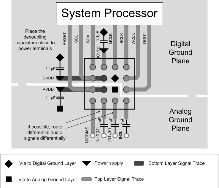
The decoupling capacitors for the power supplies must be placed close to the device terminals. Figure 44 shows the recommended decoupling capacitors for the TLV320ADC3001.
For analog differential audio signals, they must be routed differentially on the PCB for better noise immunity. Avoid crossing digital and analog signals to avoid undesirable crosstalk.
Analog and digital grounds must be separated to prevent possible digital noise from affecting the analog performance of the board.
13.2 Layout Example
 Figure 45. Layout Recommendation