ZHCSMZ7A December 2020 – June 2021 TLV320ADC5120
PRODUCTION DATA
- 1 特性
- 2 应用
- 3 说明
- 4 Revision History
- 5 Device Comparison Table
- 6 Pin Configuration and Functions
-
7 Specifications
- 7.1 Absolute Maximum Ratings
- 7.2 ESD Ratings
- 7.3 Recommended Operating Conditions
- 7.4 Thermal Information
- 7.5 Electrical Characteristics
- 7.6 Timing Requirements: I2C Interface
- 7.7 Switching Characteristics: I2C Interface
- 7.8 Timing Requirements: TDM, I2S or LJ Interface
- 7.9 Switching Characteristics: TDM, I2S or LJ Interface
- 7.10 Timing Requirements: PDM Digital Microphone Interface
- 7.11 Switching Characteristics: PDM Digital Microphone Interface
- 7.12 Timing Diagrams
- 7.13 Typical Characteristics
-
8 Detailed Description
- 8.1 Overview
- 8.2 Functional Block Diagram
- 8.3
Feature Description
- 8.3.1 Serial Interfaces
- 8.3.2 Phase-Locked Loop (PLL) and Clock Generation
- 8.3.3 Input Channel Configurations
- 8.3.4 Reference Voltage
- 8.3.5 Programmable Microphone Bias
- 8.3.6
Signal-Chain Processing
- 8.3.6.1 Programmable Channel Gain and Digital Volume Control
- 8.3.6.2 Programmable Channel Gain Calibration
- 8.3.6.3 Programmable Channel Phase Calibration
- 8.3.6.4 Programmable Digital High-Pass Filter
- 8.3.6.5 Programmable Digital Biquad Filters
- 8.3.6.6 Programmable Channel Summer and Digital Mixer
- 8.3.6.7
Configurable Digital Decimation Filters
- 8.3.6.7.1
Linear Phase Filters
- 8.3.6.7.1.1 Sampling Rate: 7.35 kHz to 8 kHz
- 8.3.6.7.1.2 Sampling Rate: 14.7 kHz to 16 kHz
- 8.3.6.7.1.3 Sampling Rate: 22.05 kHz to 24 kHz
- 8.3.6.7.1.4 Sampling Rate: 29.4 kHz to 32 kHz
- 8.3.6.7.1.5 Sampling Rate: 44.1 kHz to 48 kHz
- 8.3.6.7.1.6 Sampling Rate: 88.2 kHz to 96 kHz
- 8.3.6.7.1.7 Sampling Rate: 176.4 kHz to 192 kHz
- 8.3.6.7.1.8 Sampling Rate: 352.8 kHz to 384 kHz
- 8.3.6.7.1.9 Sampling Rate: 705.6 kHz to 768 kHz
- 8.3.6.7.2 Low-Latency Filters
- 8.3.6.7.3
Ultra-Low Latency Filters
- 8.3.6.7.3.1 Sampling Rate: 14.7 kHz to 16 kHz
- 8.3.6.7.3.2 Sampling Rate: 22.05 kHz to 24 kHz
- 8.3.6.7.3.3 Sampling Rate: 29.4 kHz to 32 kHz
- 8.3.6.7.3.4 Sampling Rate: 44.1 kHz to 48 kHz
- 8.3.6.7.3.5 Sampling Rate: 88.2 kHz to 96 kHz
- 8.3.6.7.3.6 Sampling Rate: 176.4 kHz to 192 kHz
- 8.3.6.7.3.7 Sampling Rate: 352.8 kHz to 384 kHz
- 8.3.6.7.1
Linear Phase Filters
- 8.3.7 Dynamic Range Enhancer (DRE)
- 8.3.8 Dynamic Range Compressor (DRC)
- 8.3.9 Automatic Gain Controller (AGC)
- 8.3.10 Voice Activity Detection (VAD)
- 8.3.11 Digital PDM Microphone Record Channel
- 8.3.12 Interrupts, Status, and Digital I/O Pin Multiplexing
- 8.4 Device Functional Modes
- 8.5 Programming
- 8.6 Register Maps
- 9 Application and Implementation
- 10Power Supply Recommendations
- 11Layout
- 12Device and Documentation Support
- 13Mechanical, Packaging, and Orderable Information
7.13 Typical Characteristics
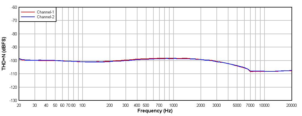
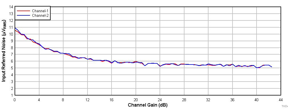
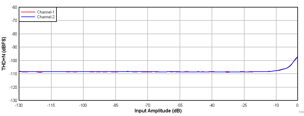
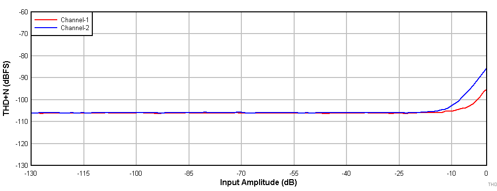
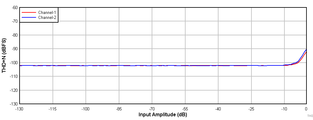
at TA = 25°C, AVDD = 3.3 V, IOVDD = 3.3 V, fIN = 1-kHz sinusoidal signal, fS = 48 kHz, 32-bit audio data, BCLK = 256 × fS, TDM slave mode, PLL on, DRE_LVL = –36 dB, channel gain = 0 dB, and linear phase decimation filter (unless otherwise noted); all performance measurements are done with a 20-kHz, low-pass filter, and an A-weighted filter
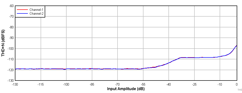
| Differential input |
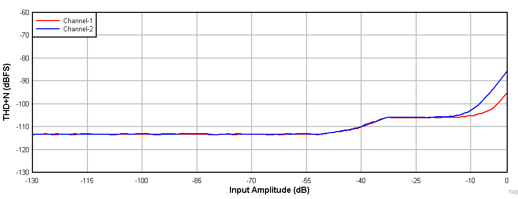
| Single-ended input |
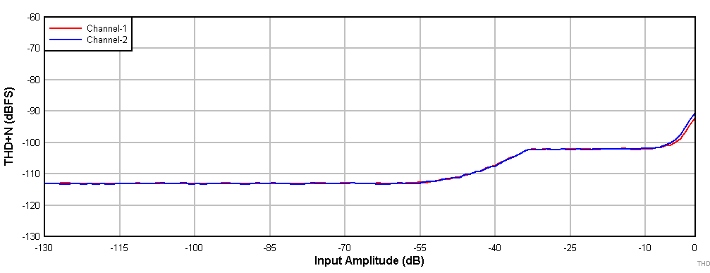
| Differential input with AVDD = 1.8 V and VREF = 1.375 V |
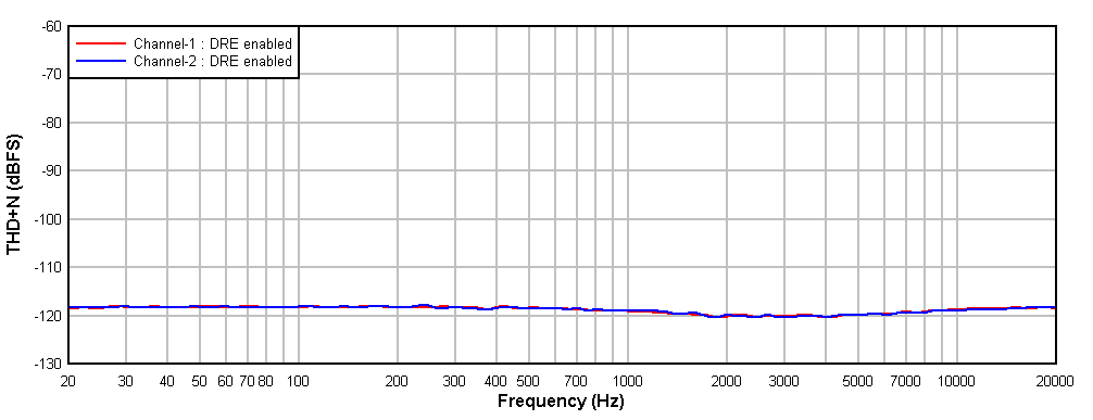
| Single-ended input |
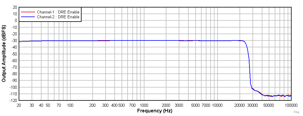 Figure 7-16 Frequency Response With a –30-dBr Input
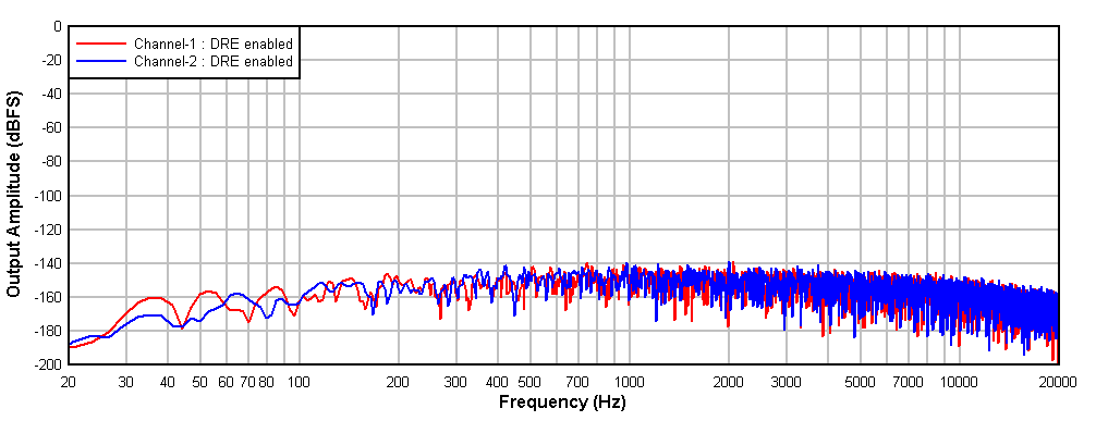 Figure 7-18 FFT
With Idle Input With DRE Enabled
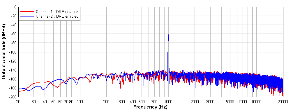 Figure 7-20 FFT
With a –60-dBr Input
With DRE Enabled
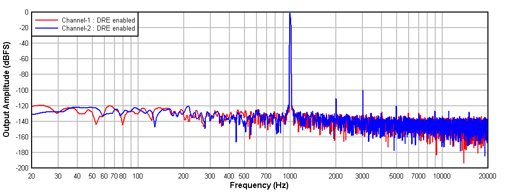 Figure 7-22 FFT
With a –1-dBr Input With
DRE Enabled
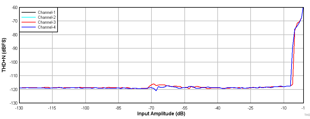 Figure 7-24 PDM Input THD+N vs Input Amplitude
 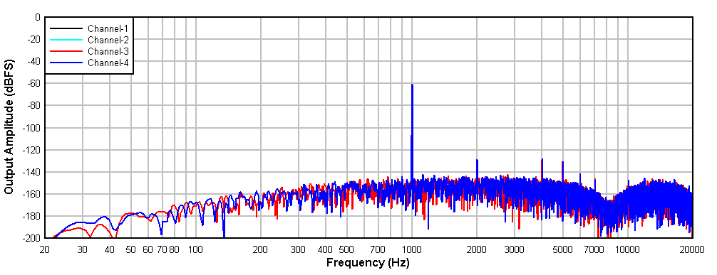 Figure 7-26 PDM
Input FFT With a –60-dBr Input
| Differential input |
| Single-ended input |
| Differential input with AVDD = 1.8 V and VREF = 1.375 V |
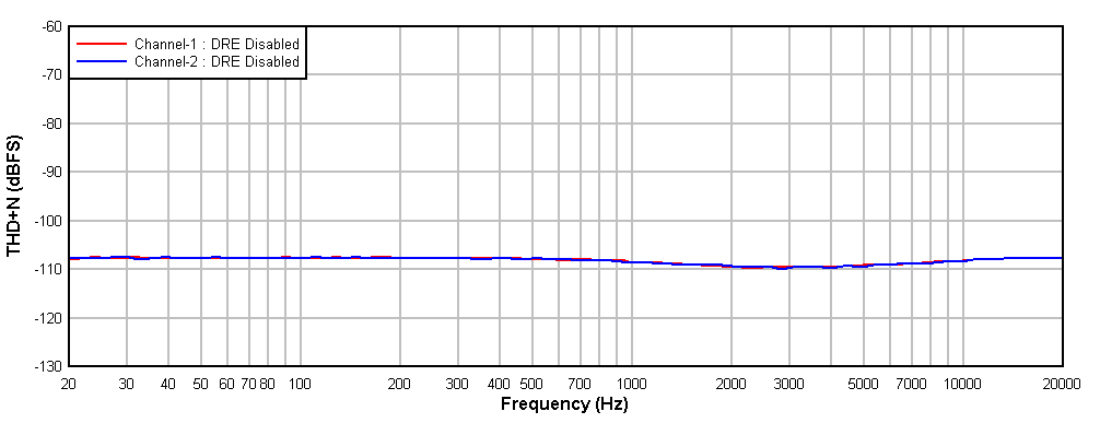
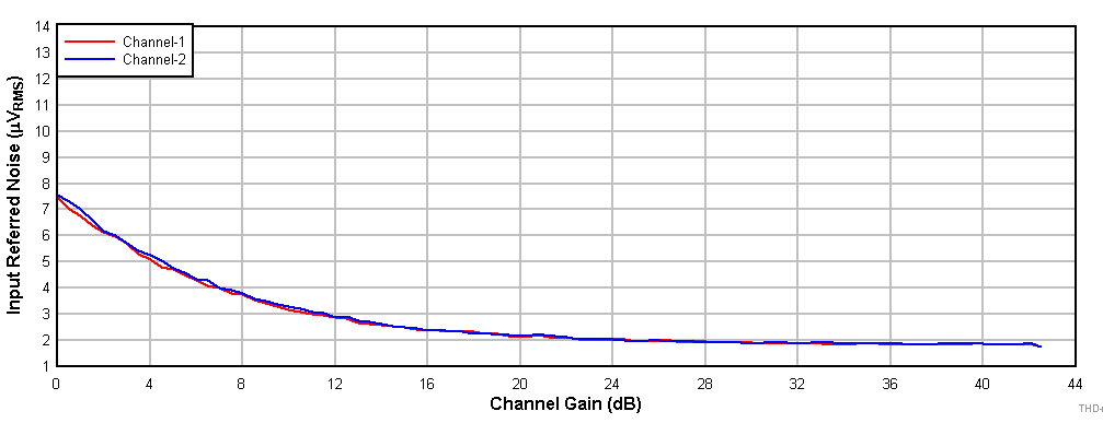
| Differential input |
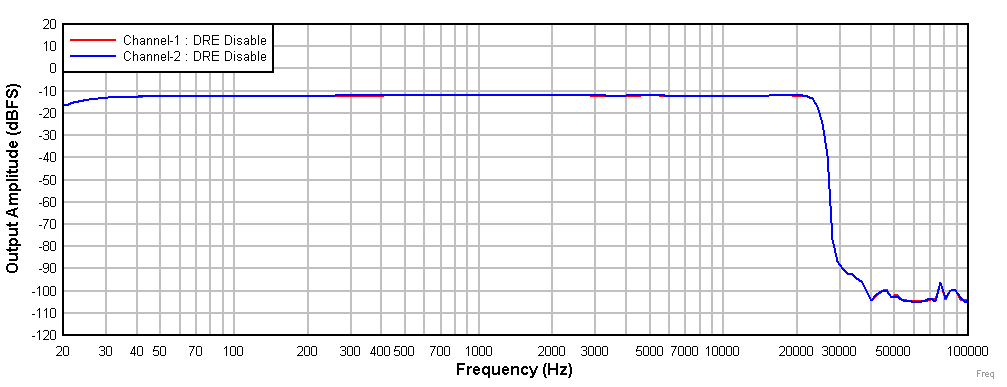
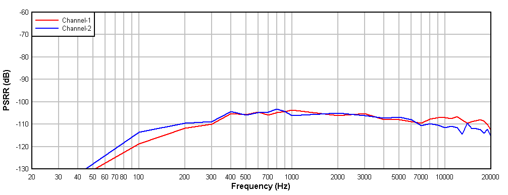 Figure 7-17 Power-Supply Rejection Ratio vs Ripple Frequency With 100-mVPP
Amplitude
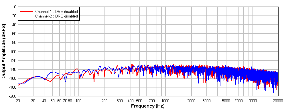 Figure 7-19 FFT
With Idle Input With DRE
Disabled
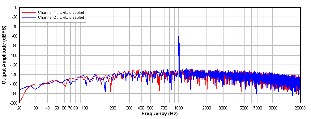 Figure 7-21 FFT
With a –60-dBr Input
With DRE Disabled
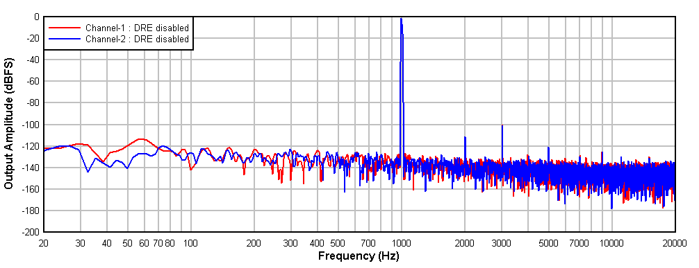 Figure 7-23 FFT
With a –1-dBr Input With
DRE Disabled
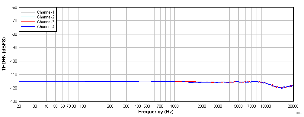 Figure 7-25 PDM
Input THD+N vs Input Frequency With a
 –20-dBr Input
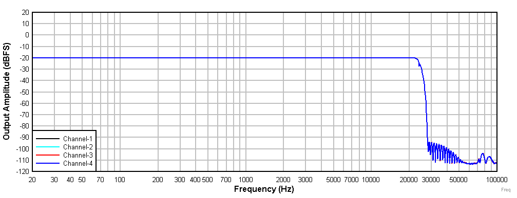 Figure 7-27 PDM
Input Frequency Response With a
 –20-dBr Input