ZHCSRJ6D June 2010 – October 2024 TLV320AIC3104-Q1
PRODUCTION DATA
- 1
- 1 特性
- 2 应用
- 3 说明
- 4 Device Comparison
- 5 Pin Configuration and Functions
-
6 Specifications
- 6.1 Absolute Maximum Ratings
- 6.2 ESD Ratings
- 6.3 Recommended Operating Conditions
- 6.4 Thermal Information
- 6.5 Electrical Characteristics
- 6.6 Switching Characteristics I2S/LJF/RJF Timing in Master Mode
- 6.7 Switching Characteristics I2S/LJF/RJF Timing in Slave Mode
- 6.8 Switching Characteristics DSP Timing in Master Mode
- 6.9 Switching Characteristics DSP Timing in Slave Mode
- 6.10 Typical Characteristics
-
7 Detailed Description
- 7.1 Overview
- 7.2 Functional Block Diagram
- 7.3
Feature Description
- 7.3.1 Audio Data Converters
- 7.3.2 Stereo Audio ADC
- 7.3.3 Automatic Gain Control (AGC)
- 7.3.4 Stereo Audio DAC
- 7.3.5 Digital Audio Processing for Playback
- 7.3.6 Digital Interpolation Filter
- 7.3.7 Delta-Sigma Audio DAC
- 7.3.8 Audio DAC Digital Volume Control
- 7.3.9 Analog Output Common-mode Adjustment
- 7.3.10 Audio DAC Power Control
- 7.3.11 Audio Analog Inputs
- 7.3.12 Analog Input Bypass Path Functionality
- 7.3.13 ADC PGA Signal Bypass Path Functionality
- 7.3.14 Input Impedance and VCM Control
- 7.3.15 MICBIAS Generation
- 7.3.16 Analog Fully Differential Line Output Drivers
- 7.3.17 Analog High-Power Output Drivers
- 7.3.18 Short-Circuit Output Protection
- 7.3.19 Jack and Headset Detection
- 7.4 Device Functional Modes
- 7.5 Programming
- 8 Register Maps
- 9 Application and Implementation
- 10Device and Documentation Support
- 11Revision History
- 12Mechanical, Packaging, and Orderable Information
7.5.9 TDM Data Transfer
Time-division multiplexed data transfer can be realized in any of the left- transfer modes if the 256-clock bit-clock mode is selected, although it is recommended to be used in either left-justified mode or DSP mode. By changing the programmable offset, the bit clock in each frame where the data begins can be changed, and the serial data output driver (DOUT) can also be programmed to the high-impedance state during all bit clocks except when valid data is being put onto the bus. This allows other codecs to be programmed with different offsets and to drive their data onto the same DOUT line, just in a different slot. For incoming data, the codec simply ignores data on the bus except where it is expected, based on the programmed offset.
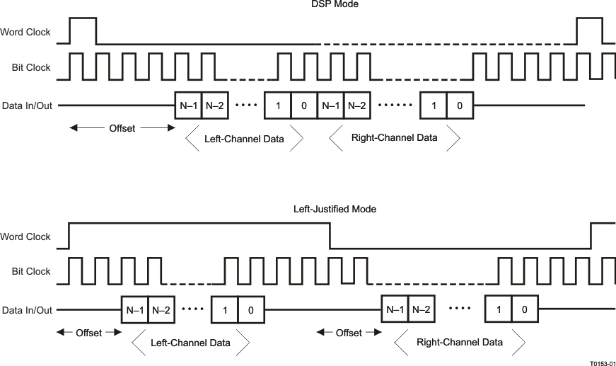
Note that the location of the data when an offset is programmed is different, depending on what transfer mode is selected. In DSP mode, both left and right channels of data are transferred immediately adjacent to each other in the frame. This differs from left-justified mode, where the left- and right-channel data are always a half-frame apart in each frame. In this case, as the offset is programmed from zero to some higher value, both the left- and right-channel data move across the frame, but still stay a full half-frame apart from each other. This is depicted in Figure 7-20 for the two cases.
 Figure 7-20 DSP Mode and Left-Justified Mode, Showing the Effect of a Programmed Data-Word Offset